

Printed board and method of displaying an identification mark on the same
- Summary
- Abstract
- Description
- Claims
- Application Information
AI Technical Summary
Benefits of technology
Problems solved by technology
Method used
Image

Examples
Embodiment Construction
[0026] An embodiment of the invention is described in detail hereinafter. However, the embodiment of the invention described hereinafter is preferred specific examples for carrying out the invention, and various technical limitations are made thereto, but it is to be pointed out that the invention is not limited thereto unless specifically and explicitly described otherwise in the following description.
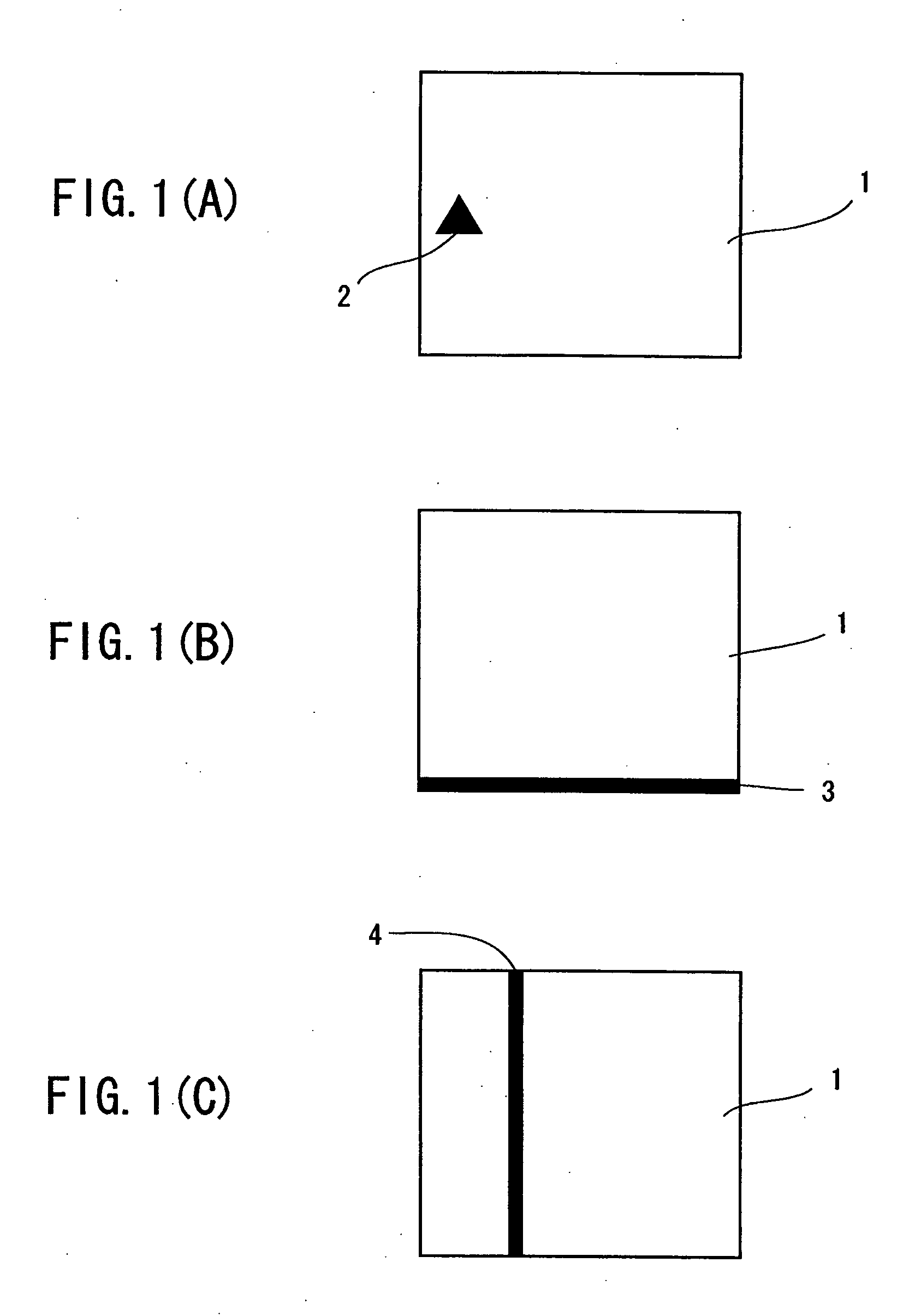
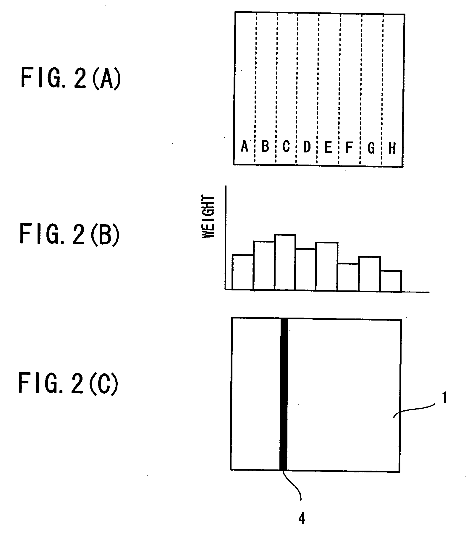
[0027]FIG. 1 is a schematic plan view showing the embodiment of the invention. Identification marks 2 to 4, each are displayed on the upper surface of a printed board 1. Circuit components mounted on the printed board 1 are omitted for brevity in explanation. In FIG. 1(A), the identification mark 2 in the shape of a triangle is displayed substantially in the central part of the printed board 1, in the vertical direction along the plane of the figure. Further, the vertex of the triangle, pointing upward, indicates that the upper half portion of the printed board 1 is lighter in weight...
PUM
 Abstract
Description
Claims
Application Information