Semiconductor device

A technology for semiconductors and devices, applied in the field of semiconductor devices, can solve the problems of the deterioration of the flatness of the wiring substrate and the reduction of reliability, and achieve the effects of excellent noise resistance, stable size and shape, and high yield

Inactive Publication Date: 2005-09-07
RENESAS ELECTRONICS CORP
View PDF0 Cites 0 Cited by
  • Summary
  • Abstract
  • Description
  • Claims
  • Application Information

AI Technical Summary

Problems solved by technology

[0013] An object of the present invention is to prevent the damage of the semiconductor chip by means of the optimization of the package external dimension, improve the reliability of the semi

Method used


Image

  • Semiconductor device
  • Semiconductor device
  • Semiconductor device

Examples


Example Embodiment

[0157] Example 1

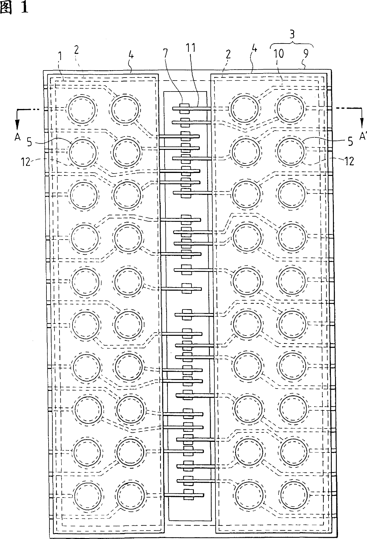
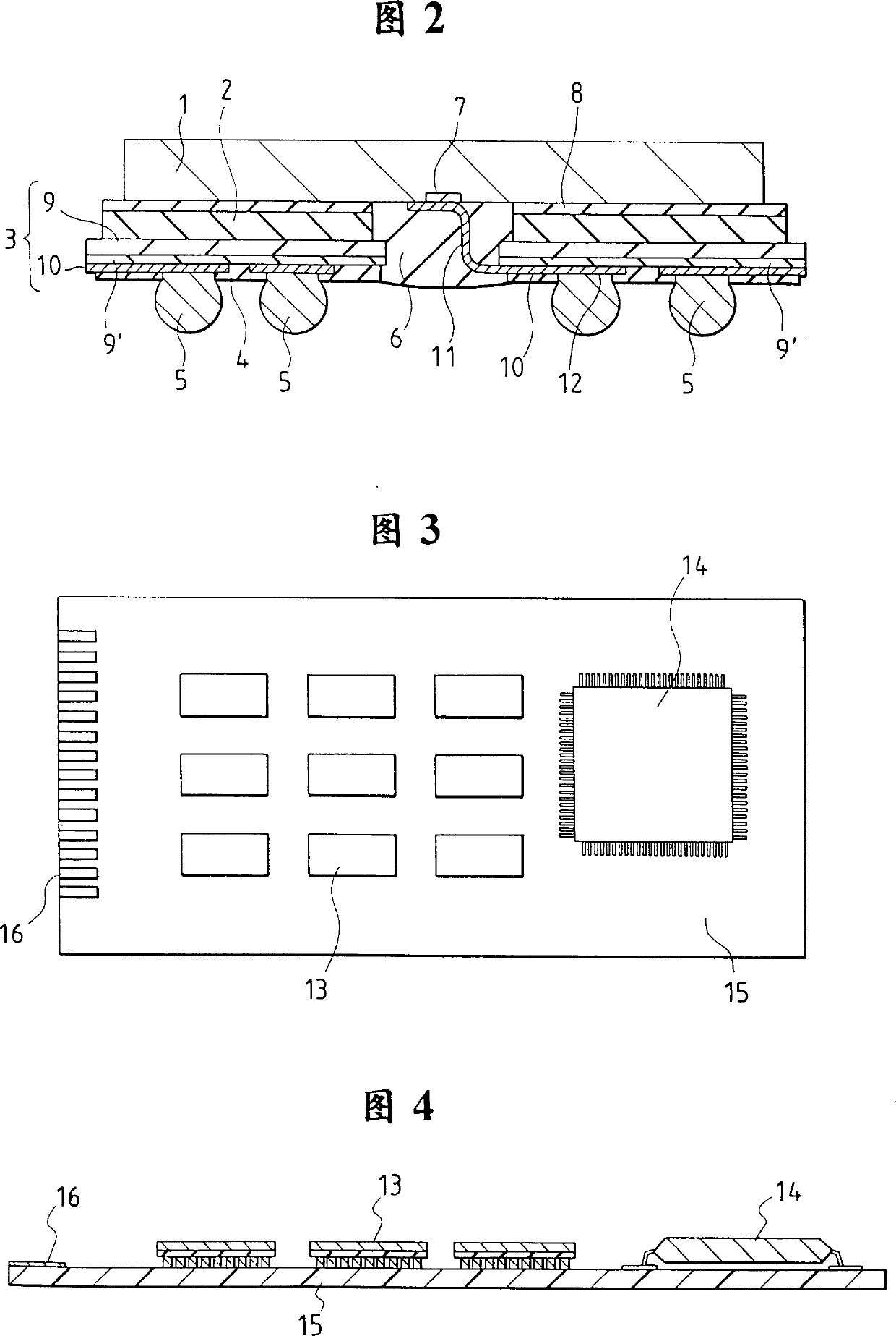
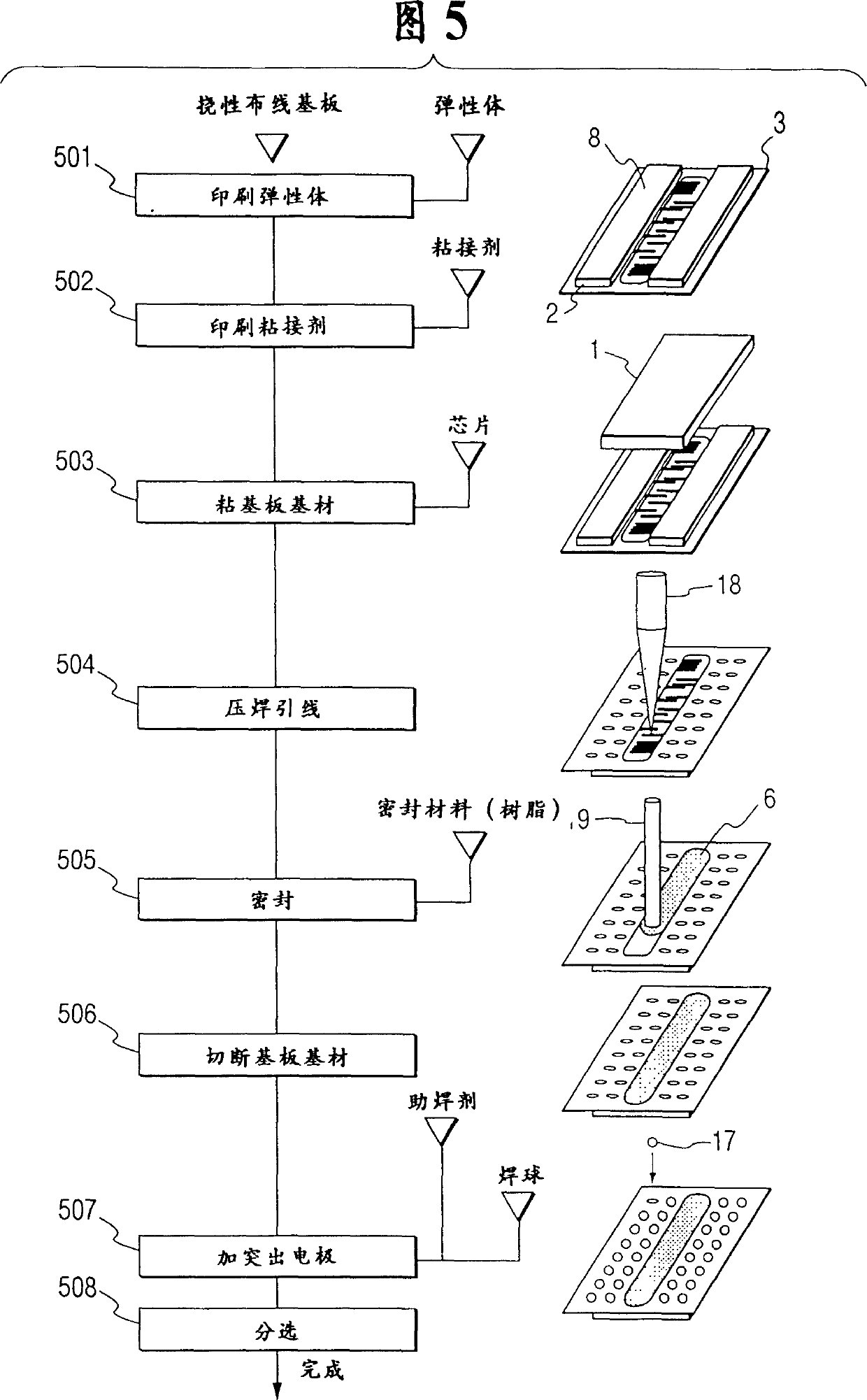
[0158] 1 is a plan view showing a semiconductor integrated circuit device according to Embodiment 1 of the present invention; FIG. 2 is a cross-sectional view taken along the line AA' of FIG. 1 ; The assembly state of the integrated circuit device on the assembly substrate; Fig. 5 shows a flowchart of the assembly process of the semiconductor integrated circuit device; Figs. 6-58, Fig. 76-Fig. An explanatory diagram illustrating a comparison between the characteristics of the circuit device and the semiconductor integrated circuit device of the comparative example examined by the present inventors. The description of these figures will be described item by item in each technical item described later.

[0159] First, the configuration of the semiconductor integrated circuit device of the first embodiment will be described with reference to FIGS. 1 and 2 .

[0160] The semiconductor integrated circuit device of the first embodiment is defined as a semiconduc...

Example Embodiment

[0293] Example 2

[0294] The semiconductor integrated circuit device of the second embodiment is a semiconductor package of the solder ball grid array type, as in the above-described first embodiment, and the difference from the above-described first embodiment is whether the technology presupposes the surface wiring structure. , but a technology that is based on the backside wiring structure and is used to improve it. For example, as shown in Figure 59 and Figure 60, the elastomer 2 that has been bonded to the main surface of the semiconductor chip 1 and will be bonded In the structure between the flexible wiring board 3 (wiring board) on the main surface of the elastic body 2 , the solder resist layer 56 (insulating film) is already formed on the back surface of the flexible wiring board 3 .

[0295] That is, the flexible wiring board 3 becomes composed of the board base material 9 to be the base material of the flexible wiring board 3 and the wiring 10 to be bonded to the ...

Example Embodiment

[0303] Example 3

[0304] 63 is a plan view of the semiconductor integrated circuit device according to Embodiment 3 of the present invention viewed from the back of the semiconductor chip; FIG. 62 is a plan view; FIG. 63 is a cross-sectional view; It is a plan view for explaining the wiring structure of the wiring board.

[0305] The semiconductor integrated circuit device of the present embodiment 3 does not use the so-called fan-in central pad structure semiconductor package as in the above-mentioned embodiments 1 and 2, but uses the peripheral pad structure as shown in FIGS. 61 to 65 instead. In the semiconductor chip 1a, the solder bump electrodes 5a connected to the bonding pads of the semiconductor chip 1a are arranged in a region from the inner side of the outer circumference of the semiconductor chip 1a to form a so-called fan-in peripheral pad. Package construction. Also, even in the third embodiment. It has also been adopted in the above-mentioned Example 1 from ...


PUM


Abstract

A ball grid array type semiconductor package includes a semiconductor chip formed with bonding pads, an elastomer bonded to the semiconductor chip, a flexible wiring substrate bonded to the elastomer and formed with wirings connected at one end of the bonding pads of the semiconductor chip, a solder resist formed on the main surface of the flexible wiring substrate and solder bump electrodes connected to the other ends of the wirings. The elastomer is bonded to the flexible wiring substrate on the side of the tape, the solder resist is formed on the side of the wirings, and the solder bump electrodes are connected with the wirings by way of through holes formed in the solder resist.

Description

technical field [0001] The present invention relates to semiconductor device technology, and particularly relates to a technology applicable and effective to portable devices such as mobile phones and portable personal computers, which have been active in the direction of small size, light weight, and thinning. Background technique [0002] In recent years, electronic equipment has been active in the direction of high functionality, high performance, small size, light weight, and thinning. In this regard, the recent rapid increase in portable devices such as portable telephones and portable personal computers plays a large role. In addition, the function of the human-machine interface of the machine operated by an individual increases, and the ease of handling and operability are increasingly emphasized. It is believed that in the future, with the advent of the true multimedia era, this tendency will become even stronger. [0003] In such a situation, there is no end to pr...

Claims


Application Information

Patent Timeline
IPC IPC(8): H01L21/60H01L21/50H01L21/98H01L23/12H01L23/28H01L23/48H01L23/495H01L23/498H01L23/50H01L27/105
CPCH01L2924/01015H01L23/4985H01L2924/01023H01L2924/0105H01L2924/01082H01L23/49827H01L2924/01004H01L2924/01002H01L2224/73215H01L2924/15311H01L2924/01029H01L2224/0401H01L2224/85951H01L2224/48472H01L2224/06136H01L2924/014H01L2924/01013H01L2224/45147H01L24/06H01L24/48H01L2924/01079H01L2224/48465H01L2224/04042H01L2924/14H01L2924/01005H01L2924/01033H01L2924/01006H01L23/49816H01L2924/01078H01L24/50H01L2924/01014H01L2924/01057H01L2224/45144H01L24/45H01L24/86H01L2224/05554H01L2224/45015H01L2224/45124H01L2224/50H01L2924/00011H01L2924/00014Y10T29/4913Y10T29/49169H01L2924/20753H01L2224/05599H01L23/28
Inventor 宫崎忠一秋山雪治柴本正训下石智明安生一郎西邦彦西村朝雄田中英树木本良辅坪崎邦宏长谷部昭男
Owner RENESAS ELECTRONICS CORP
Why Eureka
Try Eureka