Thin film array panel

Inactive Publication Date: 2005-05-12
SAMSUNG DISPLAY CO LTD
View PDF8 Cites 7 Cited by
  • Summary
  • Abstract
  • Description
  • Claims
  • Application Information

AI Technical Summary

Benefits of technology

[0017] The first and the second projections may fully overlap the first and the data lines, respectively, or have a width smaller than width of the f

Problems solved by technology

However, the signal lines may make parasitic capacitances that deteriorate image quality.
The difference of the parasitic capacitances may make the image quality worse.

Method used


Image

  • Thin film array panel
  • Thin film array panel
  • Thin film array panel

Examples


Embodiment Construction

[0024] The present invention now will be described more fully hereinafter with reference to the accompanying drawings, in which preferred embodiments of the invention are shown. The present invention may, however, be embodied in many different forms and should not be construed as limited to the embodiments set forth herein.

[0025] In the drawings, the thickness of layers, films and regions are exaggerated for clarity. Like numerals refer to like elements throughout. It will be understood that when an element such as a layer, film, region or substrate is referred to as being “on” another element, it can be directly on the other element or intervening elements may also be present. In contrast, when an element is referred to as being “directly on” another element, there are no intervening elements present.

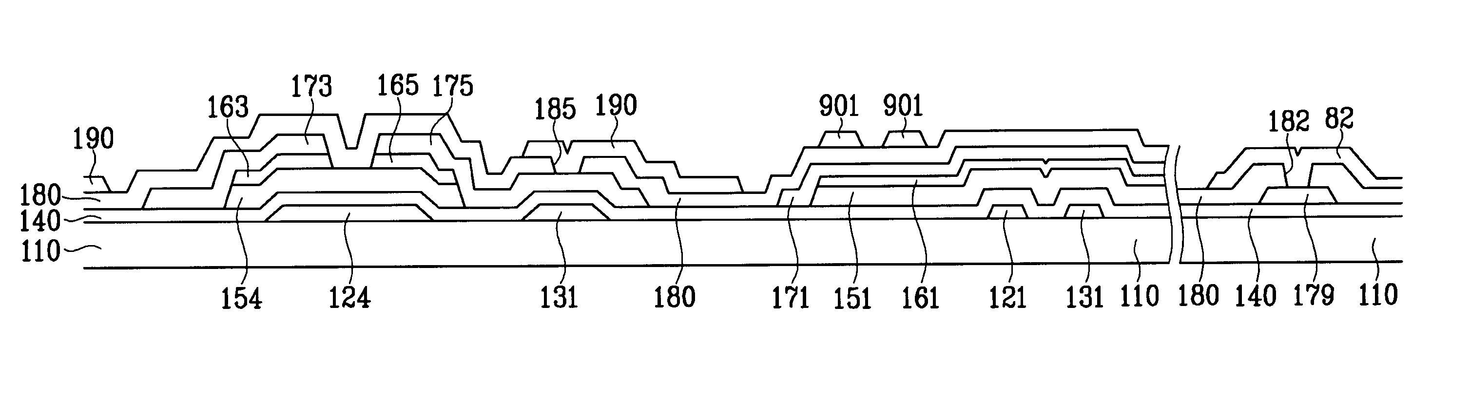
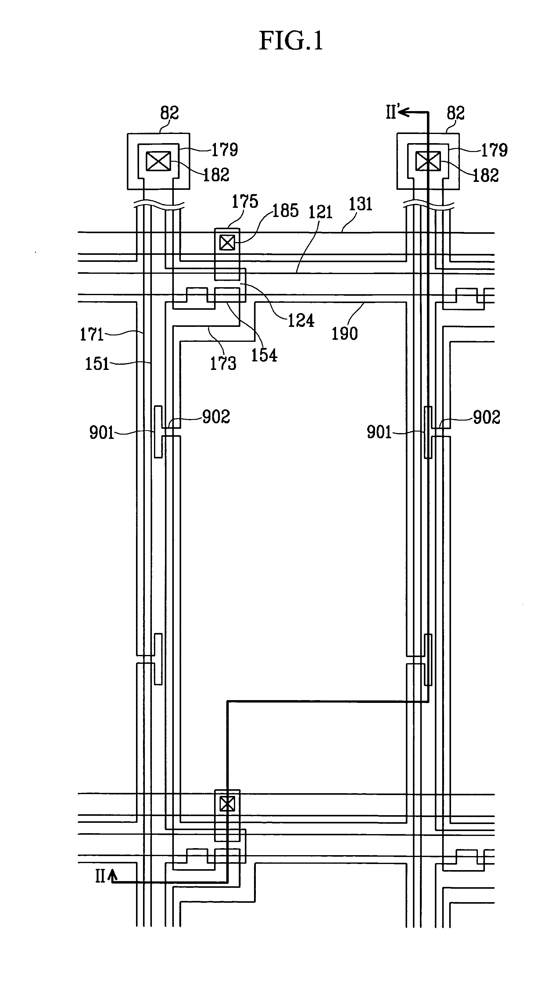
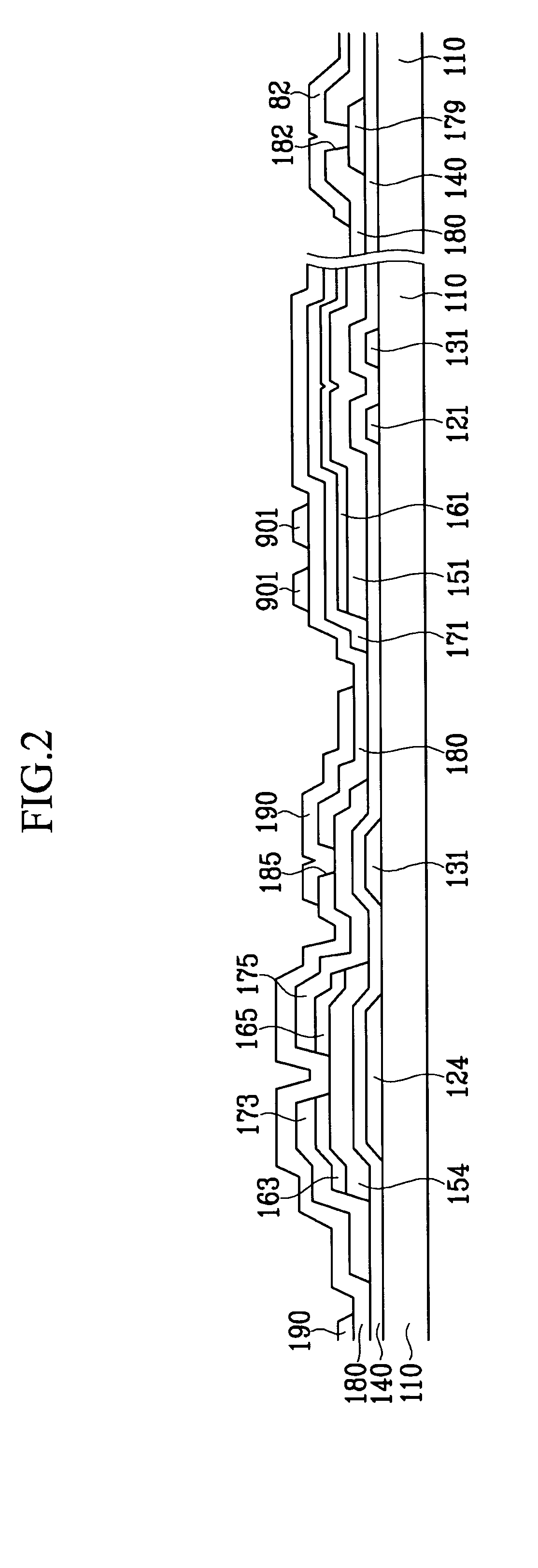
[0026] Now, TFT array panels and manufacturing methods thereof according to embodiments of the present invention will be described with reference to the accompanying drawings.

[0027]...


PUM


Abstract

A thin film transistor array panel is provided, which includes: a gate line; first and second data lines insulated from the gate line; a thin film transistor connected to the gate line and the first data line; a pixel electrode disposed between the first data line and the second data line, spaced apart from the first and the second data lines, and coupled to the thin film transistor; and first and second projections connected to the pixel electrode and overlapping the first and the second data lines, respectively.

Description

BACKGROUND OF THE INVENTION [0001] (a) Field of the Invention [0002] The present invention relates to a thin film array panel. [0003] (b) Description of the Related Art [0004] Generally, a thin film array panel is used for display devices such as liquid crystal displays (LCDs) and organic light emitting displays (OLED). [0005] The LCD is one of the most widely used flat panel displays. The general structure of an LCD consists of a liquid crystal (LC) layer that is positioned between a pair of panels including field generating electrodes and polarizers. The LC layer is subjected to an electric field generated by the electrodes and variations in the field strength change the molecular orientation of the LC layer. For example, upon application of an electric field, the molecules of the LC layer change their orientation to change the polarization of light passing through the LC layer. Appropriately positioned polarizing filters selectively block the polarized light, creating bright and ...

Claims


Application Information

Patent Timeline
IPC IPC(8): G02F1/1362H01L27/12G02F1/136
CPCG02F1/136213G02F1/136286H01L27/12G02F2201/123G02F2001/13606G02F1/13606G02F1/136
Inventor PARK, MYUNG-JAEKONG, HYANG-SHIKRHEE, YOUNG-JOONPARK, HYEONG-JUN
Owner SAMSUNG DISPLAY CO LTD
Why Eureka
Try Eureka