Load-lock technique
a technology of loading and sealing chambers, applied in the direction of conveying, transportation and packaging, coatings, etc., can solve the problems of reducing the time required for the process itself, affecting the production yield, and affecting the quality of the product, so as to reduce or suppress the contamination or temperature drop
- Summary
- Abstract
- Description
- Claims
- Application Information
AI Technical Summary
Benefits of technology
Problems solved by technology
Method used
Image

Examples
embodiment 1
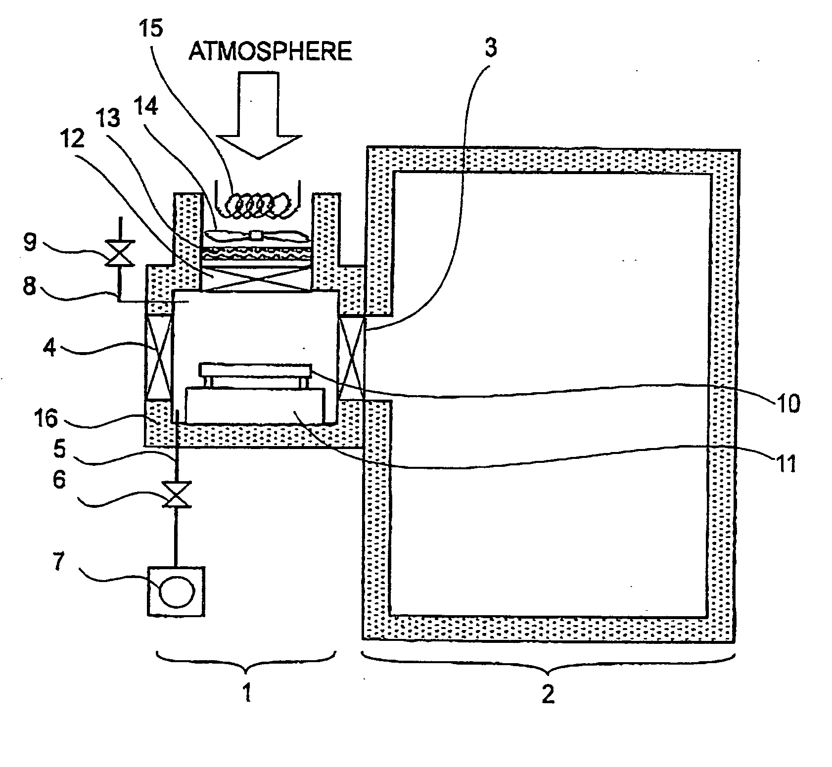
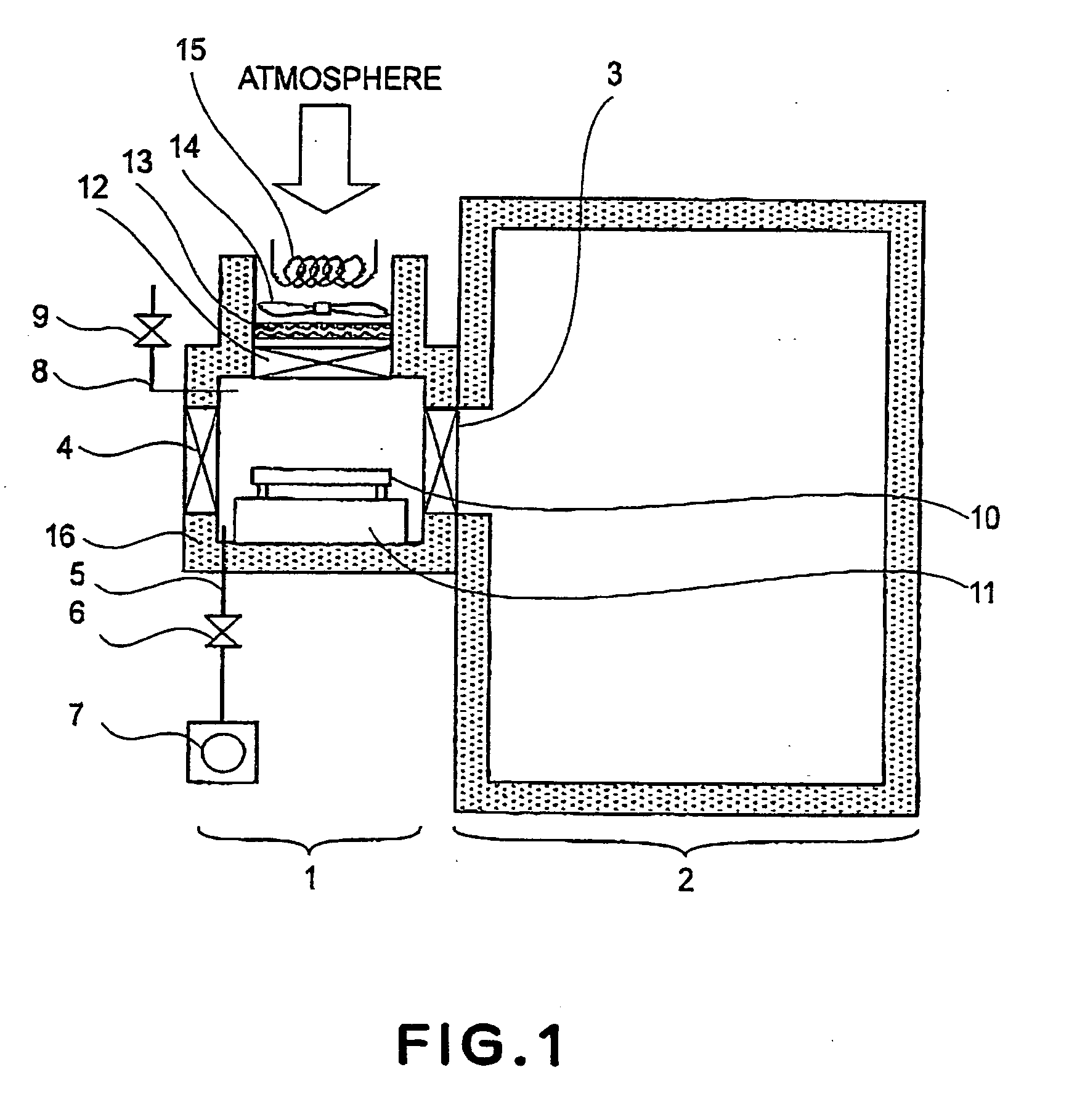
[0033]FIG. 1 illustrates a load-lock system according to a first embodiment of the present invention. The first embodiment is applied to an EUV (extreme ultraviolet) exposure apparatus wherein exposure is carried out in a vacuum ambience. Denoted at 1 is the load-lock system of the present invention, and denoted at 2 is a main chamber which is used as an exposure chamber of the exposure apparatus. The main chamber is filled with a vacuum ambience or a particular ambience such as reduced pressure He, for example. The load-lock chamber 1 serves to enable loading a substrate 10 thereinto from the atmosphere without breaking the vacuum ambience or particular ambience, and also to assure unloading the substrate 10, after being processed inside the main chamber 2, outwardly.
[0034] Basically, the present invention is directed to a load-lock system, and it is not always necessary that the machine placed at the main chamber side of the load-lock system is an exposure apparatus. It may be an...
embodiment 2
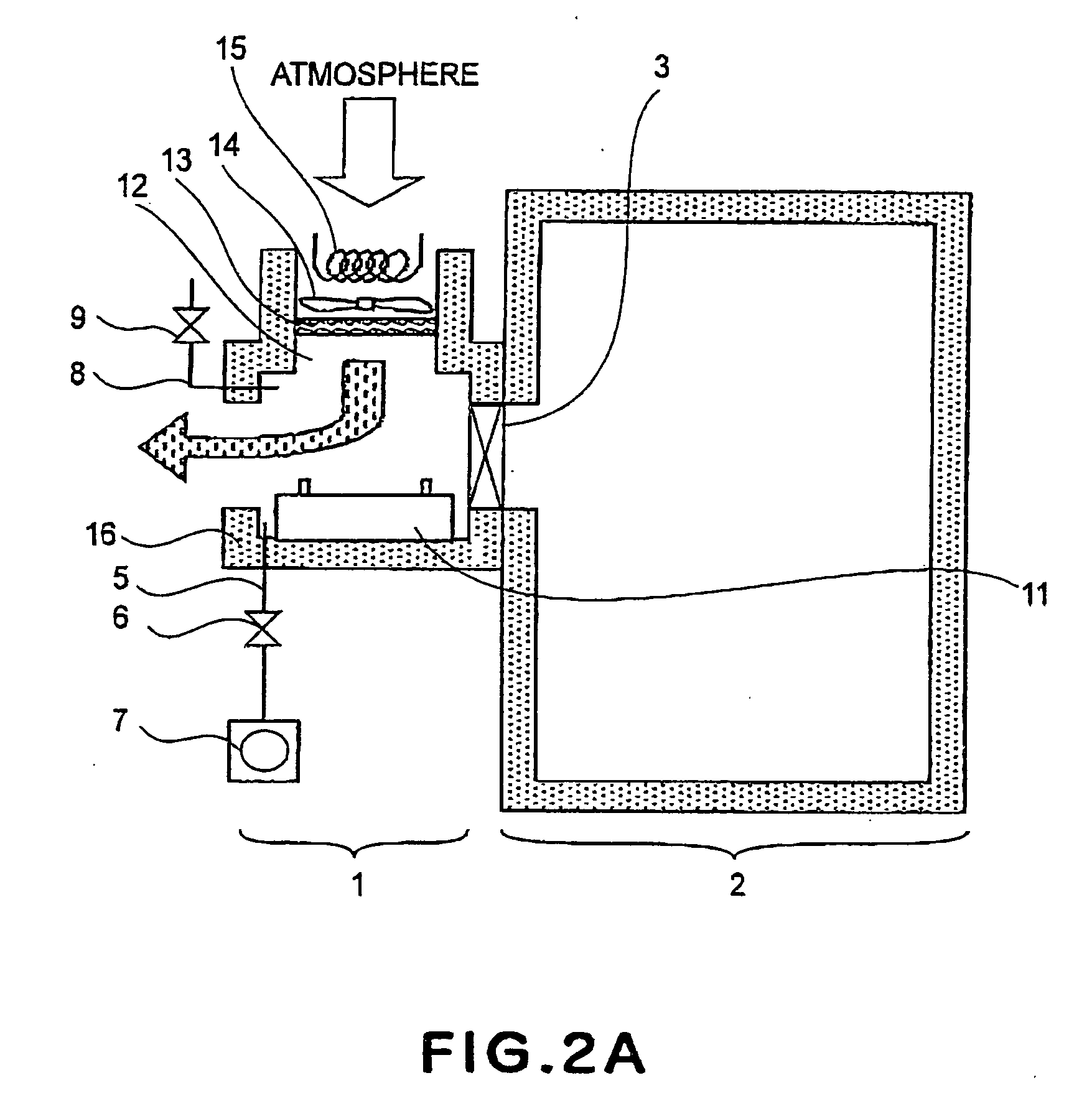
[0045]FIG. 3 illustrates a load-lock system according to a second embodiment of the present invention. The second embodiment is applied to an exposure apparatus such as EUV (extreme ultraviolet) exposure apparatus wherein exposure is carried out in a vacuum ambience or a particular ambience such as reduced pressure He. FIG. 3 is a plan view of the exposure apparatus, as seen from the above. Structural components having similar functions as those of the first embodiment are denoted by corresponding reference numerals. Denoted in the drawing at 1 is the load-lock system, and denoted at 2 is a main chamber that defines a place where the exposure process is to be carried out.
[0046] Denoted at 16 is a load-lock chamber which is a major component of the load-lock system 1. Denoted at 3 is a vacuum side gate valve, and denoted at 4 is an atmosphere side gate valve. These valves function to define an opening for passage of a substrate 10 between the load-lock chamber 16 and the main chambe...
third embodiment
[0068] Next, an embodiment of a device manufacturing method which uses an exposure apparatus described above, will be explained.
[0069]FIG. 7 is a flow chart for explaining the overall procedure for semiconductor manufacture. Step 1 is a design process for designing a circuit of a semiconductor device. Step 2 is a process for making a mask on the basis of the circuit pattern design. Step 3 is a process for preparing a wafer by using a material such as silicon. Step 4 is a wafer process which is called a pre-process wherein, by using the thus prepared mask and wafer, a circuit is formed on the wafer in practice, in accordance with lithography. Step 5 subsequent to this is an assembling step which is called a post-process wherein the wafer having been processed at step 4 is formed into semiconductor chips. This step includes an assembling (dicing and bonding) process and a packaging (chip sealing) process. Step 6 is an inspection step wherein an operation check, a durability check an ...
PUM
| Property | Measurement | Unit |
|---|---|---|
| Exposure limit | aaaaa | aaaaa |
Abstract
Description
Claims
Application Information
 - R&D Engineer
- R&D Manager
- IP Professional
- Industry Leading Data Capabilities
- Powerful AI technology
- Patent DNA Extraction
Browse by: Latest US Patents, China's latest patents, Technical Efficacy Thesaurus, Application Domain, Technology Topic.
© 2024 PatSnap. All rights reserved.Legal|Privacy policy|Modern Slavery Act Transparency Statement|Sitemap