Magnetic field effect transistor, latch and method
a magnetic field effect transistor and latch technology, applied in the field of magnetic field detection, can solve the problems of substrate bias, limited improvement of sensitivity, and limit on the smallest detectable magnetic field
- Summary
- Abstract
- Description
- Claims
- Application Information
AI Technical Summary
Benefits of technology
Problems solved by technology
Method used
Image
Examples
Embodiment Construction
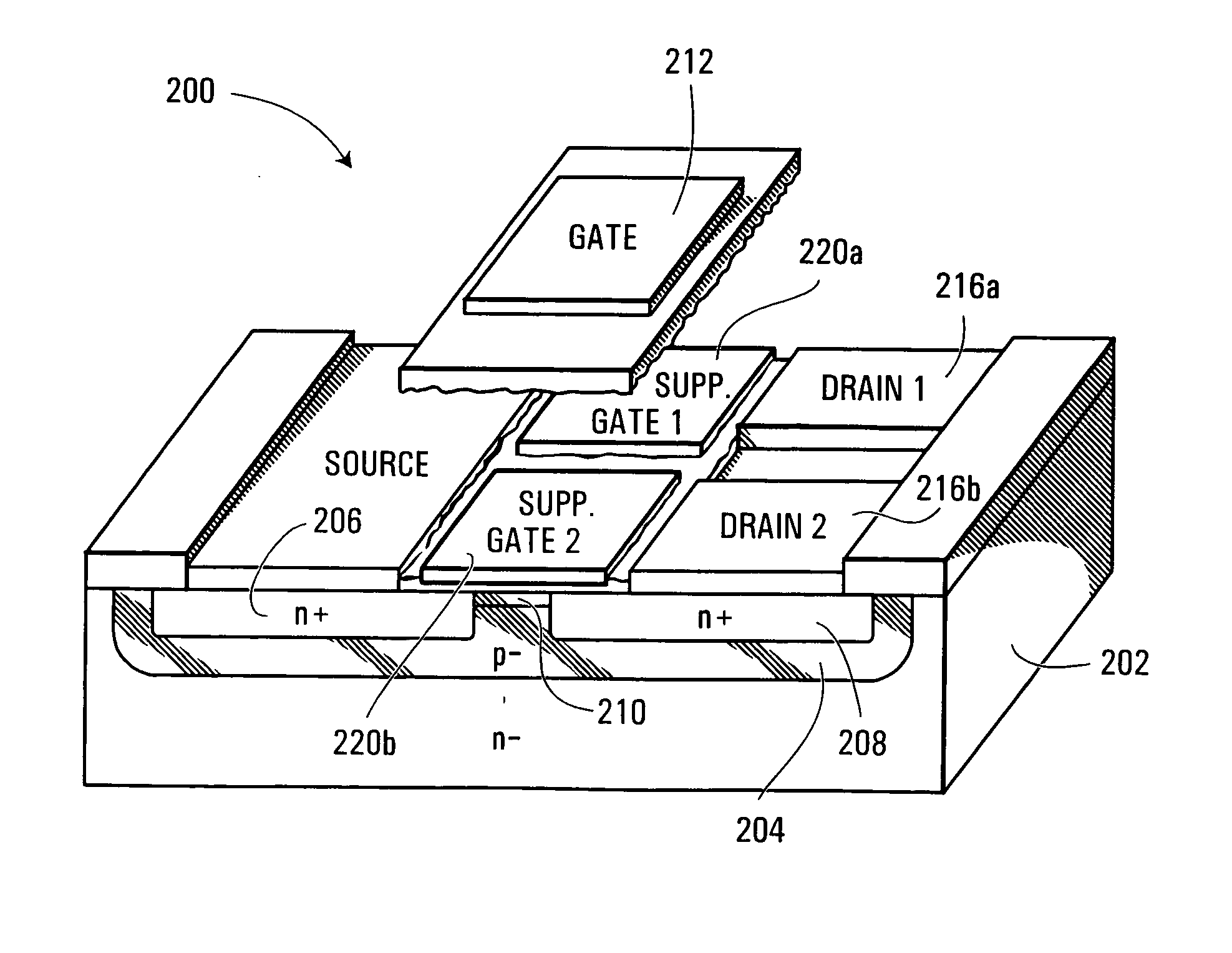
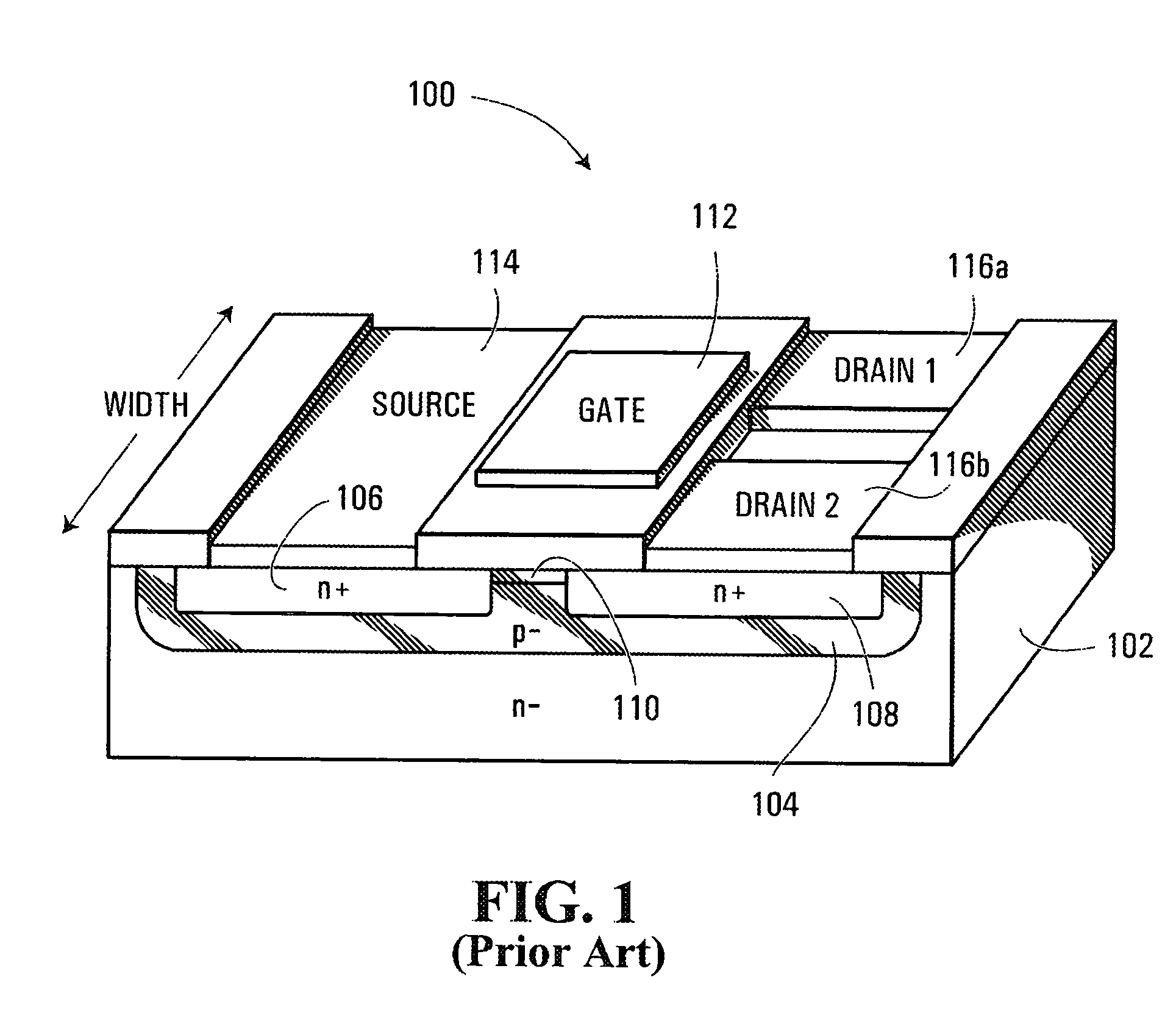
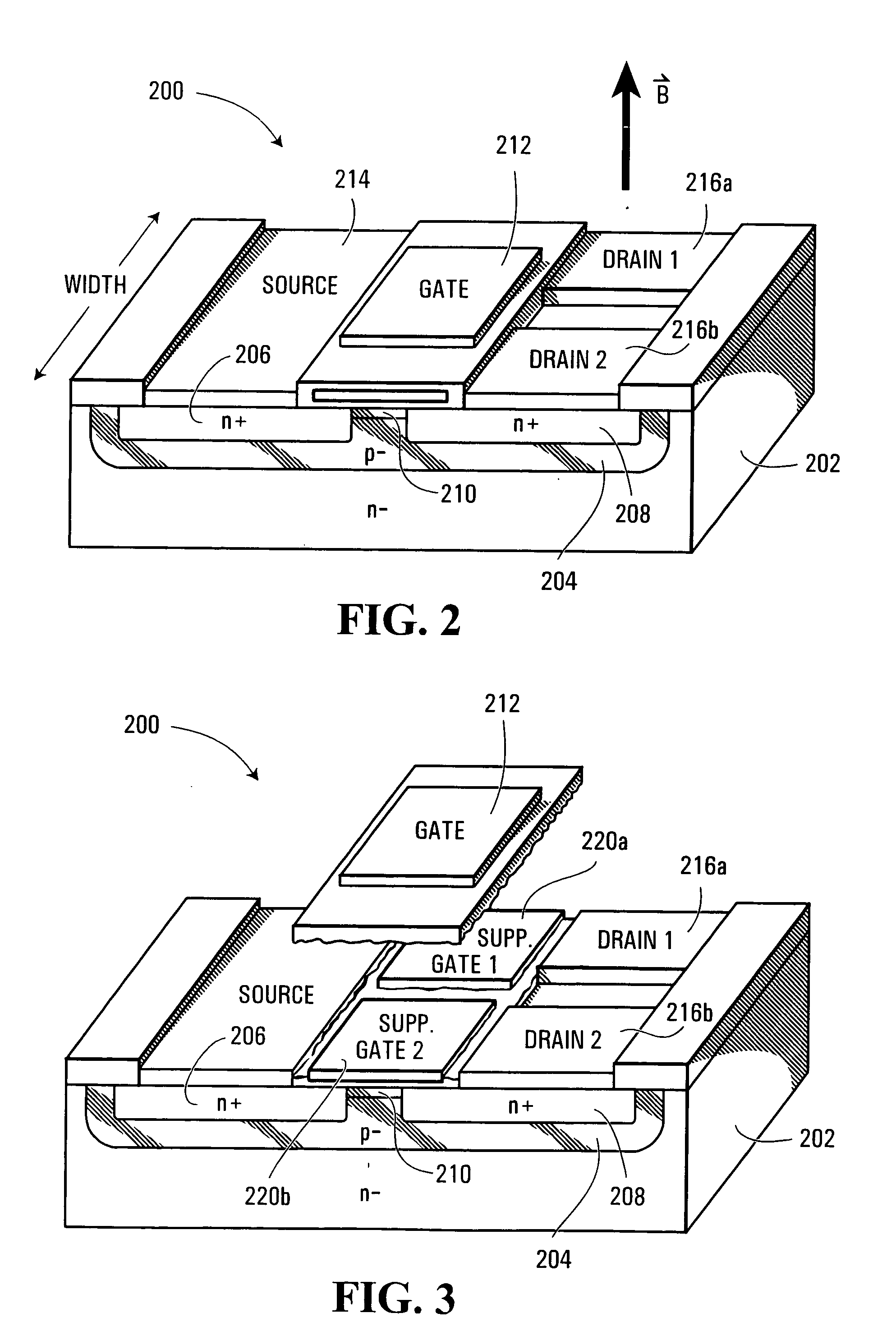
[0019]FIG. 1 illustrates a convention n-channel split drain magnetic field effect transistor (“MAGFET”) 100. As illustrated, MAGFET 100 includes a p-type semiconductor layer 104 configured as a well within a semiconductor substrate 102. Formed within layer 104 are n-type source and drain regions 106 and 108. The p-type semiconductor layer 104 extending between source and drain regions 106 and 108 defines a lengthwise extending channel 110. A conductive gate 112 is formed above channel 110. A metal contact 114 is formed atop source 106. Two laterally conductive contacts 116a and 116b are formed above drain region 108. As illustrated, contacts 116a and 116b are spaced laterally along the width of channel 110.
[0020] As will be appreciated substrate 102 could be eliminated and layer 104 could act as a p-type substrate for a suitable MAGFET.
[0021] Now, in the absence of an external magnetic field, MAGFET 100 functions in much the same way as a conventional field effect transistor. A vo...
PUM
 Abstract
Description
Claims
Application Information


