Delay circuit and control method of the delay circuit

a delay circuit and control method technology, applied in the field of delay circuits, can solve the problems of increasing the difficulty of equalizing every wiring path from an inverter gate b>400/b>, the inability to precisely control the delay control to the input signal in, and the possibility of a plurality of control signals being activated temporarily when the signal is switched over

Inactive Publication Date: 2005-08-04
SOCIONEXT INC
View PDF4 Cites 17 Cited by
  • Summary
  • Abstract
  • Description
  • Claims
  • Application Information

AI Technical Summary

Benefits of technology

[0012] Further, in the delay circuit of the conventional technology, when the control signal is changed over in the direction of increasing the amount of delay, the high level output signal of a predetermined delay unit, which is located between predetermined delay units selected before and after the switching and maintained in the non-selective state, can be propagated to the output terminal OUT, which is another problem to be solved. For example, if the input signal IN changes to high level after the control signal is switched over, a high level signal can be outputted prior to a delay signal corresponding to a proper transition signal so that a signal having an erroneous delay time can be outputted.
[0014] The present invention has been achieved to solve any one of the above-described problems of the conventional technology and an object of the present invention is to provide a delay circuit capable of controlling a delay time which should be added to the input signal accurately and switching over the delay time stably and a control method of the delay circuit.
[0017] As a result, an objective signal inputted from a first input terminal in a unit delay unit selected by a unit selection signal is provided with a unit delay time by the first and third logical portions and outputted from an output terminal. The outputted signal is inputted from the second input terminal in the unit delay unit of subsequent stages after a next stage and provided with a unit delay time by the second and third logical portions and propagated successively. Consequently, the objective signal is provided with a predetermined delay time. An unnecessary signal inputted through the second input terminal from a unit delay unit existing at a preceding stage of the unit delay unit in which the object signal is propagated is blocked from the propagation by the second logical portion. Even if the unit selection signal which should maintain its non-selective status is switched over turns to selective status temporarily due to hazard when the signal and an objective signal is propagated from a unit delay unit at an erroneous position, the propagation of the signal can be blocked at a second input terminal of the unit delay unit located at its proper selection position. Consequently, it is possible to prevent an erroneous delay signal accompanied by erroneous activation when a signal is switched from being outputted.
[0022] As evident from the above description, the present invention provides a delay circuit capable of controlling the predetermined delay time to be applied to an input signal accurately and obtaining an output signal stably when the predetermined delay time is switched over, and a control method of the delay circuit.

Problems solved by technology

Thus, there is such a problem that an output signal of a preceding stage and the input signal IN collide with each other in the NAND gates 210-410 of each stage.
Consider a case where the control signal which should maintain its inactive state is changed from this state to low level temporarily due to a hazard when the signal is switched over.
This is problematic because an erroneous delay signal is propagated to the output terminal OUT depending on the period of the erroneous activation.
Particularly, if the predetermined delay unit is constructed of multiple stages and the activation circuit of the control signal becomes complicated, the possibility that a plurality of control signals maybe activated temporarily when the signal is switched over increases.
Each time when the control signal is switched over, an unexpected signal can be outputted from the output terminal OUT, which is a problem to be solved.
Further, in the delay circuit of the conventional technology, when the control signal is changed over in the direction of increasing the amount of delay, the high level output signal of a predetermined delay unit, which is located between predetermined delay units selected before and after the switching and maintained in the non-selective state, can be propagated to the output terminal OUT, which is another problem to be solved.
Particularly, in case where the predetermined delay unit is constructed in multiple stages, it is more difficult to equalize every wiring path from an inverter gate 400.
There is such a fear that the delay control to the input signal IN cannot be controlled precisely, which is a problem to be solved.

Method used


Image

  • Delay circuit and control method of the delay circuit
  • Delay circuit and control method of the delay circuit
  • Delay circuit and control method of the delay circuit

Examples


Embodiment Construction

[0031] Hereinafter, the specific embodiment of the delay circuit and control method of the delay circuit of the present invention will be described in detail with reference to FIGS. 1-7.

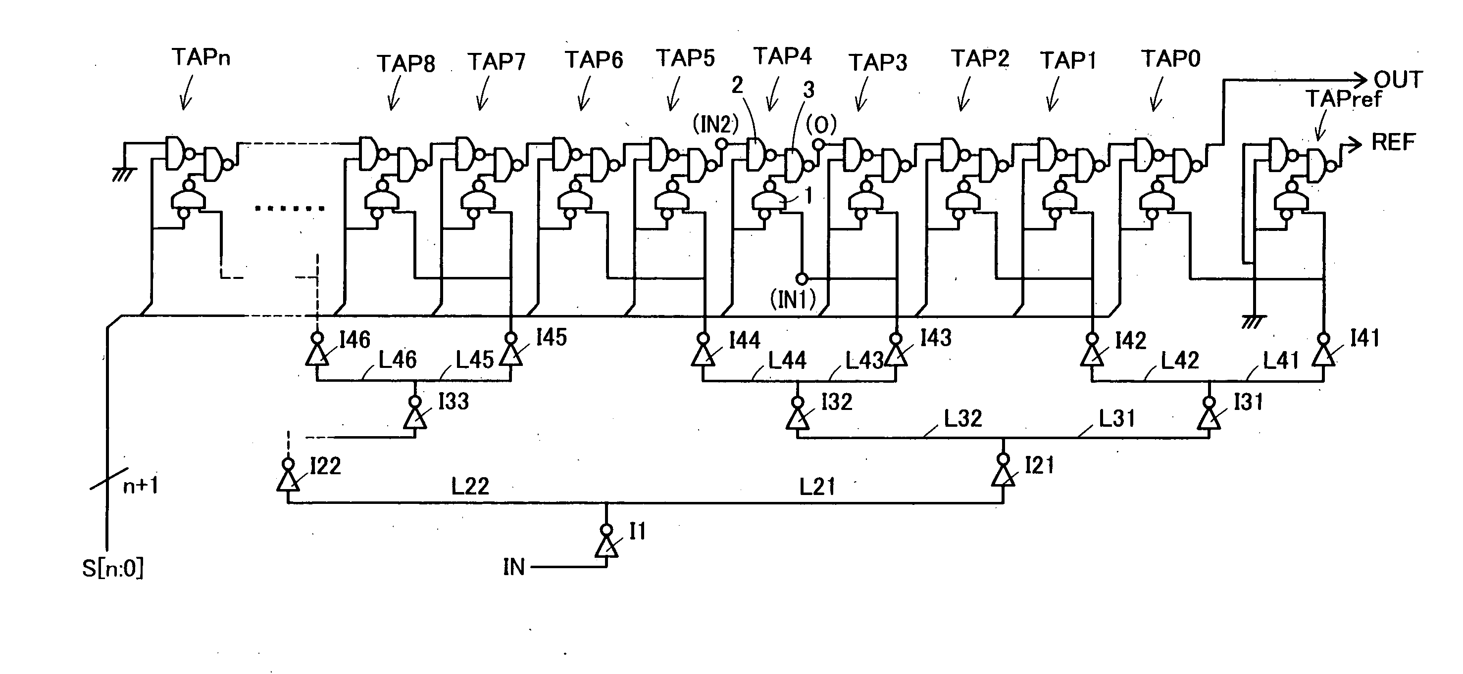
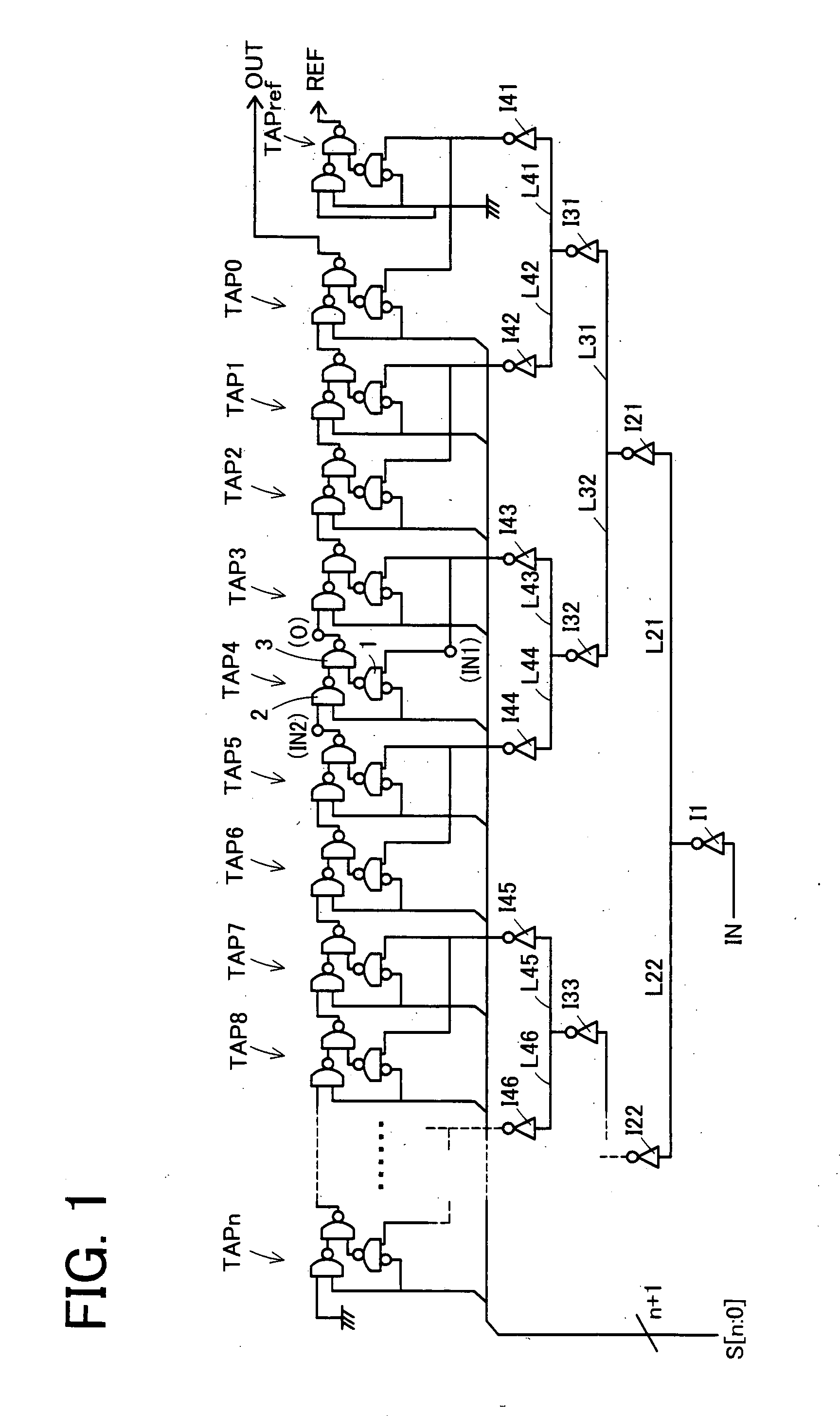
[0032]FIG. 1 shows a delay circuit of the embodiment of the present invention. In the delay circuit of the embodiment, unit delay units for applying unit delay time (τ) (hereinafter referred to as tap) TAP0-TAPn are connected in series to form multiple stages.

[0033] All the respective taps TAP0-TAPn have the same configuration. The internal structure of the tap will be described with reference to FIG. 1 by taking a tap TAP4 as an example. An objective signal for applying a predetermined delay is inputted to a signal input terminal IN1, which is an example of the first input terminal. The output terminal of a preceding stage TAP 5 is connected to a between-stages connecting terminal IN2, which is an example of the second input terminal. An output terminal 0 of the tap TAP 4 is connected to the betwe...


PUM


Abstract

A delay circuit is constructed by connecting taps TAP0-n for providing with a unit delay time (τ) in series on multiple stages. Each tap has the same configuration and an objective signal is inputted to a signal input terminal IN1. The output terminal of a preceding stage tap is connected to a between-stages connecting terminal IN2. An output terminal O is connected to the between-stages connecting terminal of a next stage tap. The signal input terminal and the between-stages connecting terminal are connected to one input terminal of NAND gates 1, 2 and a tap selection signal is inputted to the other input terminal. The output terminal is connected to a NAND gate 3. One of the NAND gates 1, 2 functions as a logical inversion gate corresponding to a tap selection signal so as to enable propagation of the signal. At this time, in the other NAND gate, the output signal is fixed to high level and the NAND gate 3 also functions as a logical inversion gate. The objective signal is propagated by the NAND gates 1, 3 and the preceding stage signal is propagated by the NAND gates 2, 3. By constructing the NAND gates 1, 2 with the same structure, the unit delay time (τ) can be matched accurately.

Description

CROSS-REFERENCE TO RELATED APPLICATIONS [0001] This application is a continuation application based upon and claims the benefit of the prior PCT International Patent Application No. PCT / JP2003 / 003640 filed on Mar. 25, 2003, the entire contents of which are incorporated herein by reference.[0002] 1. Field of the Invention [0003] The present invention relates to a delay circuit capable of adjusting the delay time of signal propagation accurately and a control method of the delay circuit. [0004] 2. Description of Related Art [0005] In recent years, the multi-function of electronic devices has progressed and a delay circuit capable of high precision delay control has been demanded for the necessity of accurately generating signals necessary for data access in, for example, an optical disk recording unit. Accompanied by the multi-function of the devices, the operating speed of semiconductor integrated circuit device has progressed to higher level. Due to the increased speed in the CPU, s...

Claims


Application Information

Patent Timeline
Patent Type & Authority Applications(United States)
IPC IPC(8): H03H11/26H03K5/00H03K5/13H03K5/15
CPCH03K5/1506H03K5/133H03K2005/00156H03K2005/00058
Inventor YAMAWAKI, MASASHI
Owner SOCIONEXT INC
Why Eureka
Try Eureka