Method of manufacturing a contact sheet and socket including same

a technology of contact sheet and socket, which is applied in the field of contact sheet, can solve the problems of increasing resistance, inability to ensure the contact load between the terminal and the contact, and inability to absorb any warp caused during contact with the electronic device, etc., and achieves wear resistance and endurance. , the effect of small resistan

Active Publication Date: 2005-10-13
NGK INSULATORS LTD
View PDF11 Cites 5 Cited by
  • Summary
  • Abstract
  • Description
  • Claims
  • Application Information

AI Technical Summary

Benefits of technology

[0023] According to a sixth embodiment of the present invention, a contact sheet is provided that is produced by bonding two of the contact sheets according to the fifth embodiment back to back to each other. In addition to the advantageous effects of the above embodiments, the effective length of the contact portion can be doubled by bonding two contact sheets back to back, sufficient displacement of each contact portion is ensured even if the terminal pitch is relatively small and the distance between electronic devices is relatively large, and the contact portion effectively conducts between corresponding terminals on each electronic device.
[0024] According to a seventh embodiment of the present invention, a method for producing a contact sheet for providing an electrical connection between the terminals of two or more electronic devices by positioning the contact sheet between the electronic devices is provided. The method includes the steps of providing a first insulative base sheet having a smaller number of first through-holes than the number of terminals of the electronic device formed therein in an arrayed pattern and providing a second insulative base sheet having a plurality of second through-holes formed therein in an arrayed pattern corresponding to the number of terminals. A metal sheet is formed into a metal contact sheet comprising a plurality of conductive contacts. Each conductive contact comprises a first fixed part which corresponds to a part of the area surrounding a respective one of the first through-holes. The total area of the fixed part and a respective first through-hole is greater than the unit grid area formed by an arrangement of the terminals of the electronic device. The contact also includes a moving part including an integral second part that is contiguous with and immediately adjacent the fixed part and an integral third contact portion that is contiguous with and immediately adjacent the second part. The moving part has a length substantially corresponding to the overall length of the first through-hole. The first base sheet and the metal contact sheet are arranged such that each fixed part corresponds to a part of the area surrounding a respective first through-hole and each moving part is located in a position corresponding to a respective first through-hole, and the first base sheet and metal contact sheet are bonded to form a bonded sheet.
[0025] Each moving part is bent so that the second part protrudes from one side of the bonded sheet and such that the third contact portion elastically extends a distance from the other side of the bonded sheet such that the third contact portion works as an elastic spring contact. The bonded sheet is cut into a plurality of individual contact units that comprise a plurality of contacts, and a plurality of the contact units are arranged side by side on the second base sheet so that the contact portions of each contact unit are located on the same side of the second base sheet and correspond to a respective terminal of the electronic device. The contact units and the second base sheet are bonded together to form a contact sheet.
[0026] According to this embodiment of the present invention, since the total area of the fixed part and the first through-hole is greater than the unit grid area, the length of the contact portion can be increased while the contact portions can also be positioned in close intervals, which is applicable to fine lead pitch devices. Furthermore, by arranging the contact units and bonding them to the second base sheet, it is possible to produce a contact sheet with contact portions that have sufficient displacement and which contact the terminals of the electronic device with a small resistance.
[0027] According to an eighth embodiment of the present invention, a method is provided for producing a contact sheet that comprises a step of bonding at least two contact sheets according to the seventh embodiment back to back to each other. According to this embodiment of the invention, in addition to the operation of the above seventh embodiment, contact sheets are provided wherein the contact portions protrude from both sides thereof by bonding the two contact sheets together back to back. Thus, the contact sheet effectively conducts between the corresponding terminals of each electronic device.
[0028] According to a ninth embodiment of the present invention, a socket is provided wherein a contact sheet according to the first to fourth embodiments is configured inside a frame. The socket in accordance with this embodiment includes contact portions that have sufficient displacement and which securely contact the terminals of an electronic device that has a fine lead pitch. Moreover, since the frame reinforces the contact sheet, the contact sheet has wear resistance and endurance for repetitive uses.

Problems solved by technology

However, according to this former way, the shorter the length of the contact is, the smaller the displacement length becomes, and it is impossible to absorb any warp caused during contact with the electronic device.
If, however, the contact length is preserved by instead reducing the width or the thickness of the contact (in order to maintain sufficient displacement length), a sufficient contact load between the terminal and the contact cannot be ensured.
Although the contact sheet according to U.S. Pat. No. 5,297,967 can absorb the warp of the electronic device due to the sufficient displacement length of its contact connecting part, the resistance increases, however, and the contact load tends to be small.
As a result, the electrical resistance becomes larger as a whole and it is difficult to decrease the circuit inductance and increase the operation speed.

Method used


Image

  • Method of manufacturing a contact sheet and socket including same
  • Method of manufacturing a contact sheet and socket including same
  • Method of manufacturing a contact sheet and socket including same

Examples


first embodiment

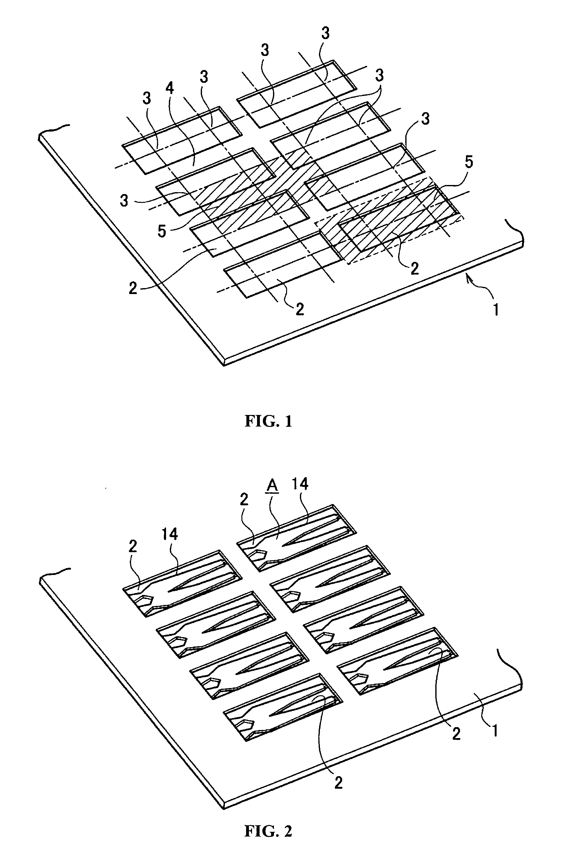
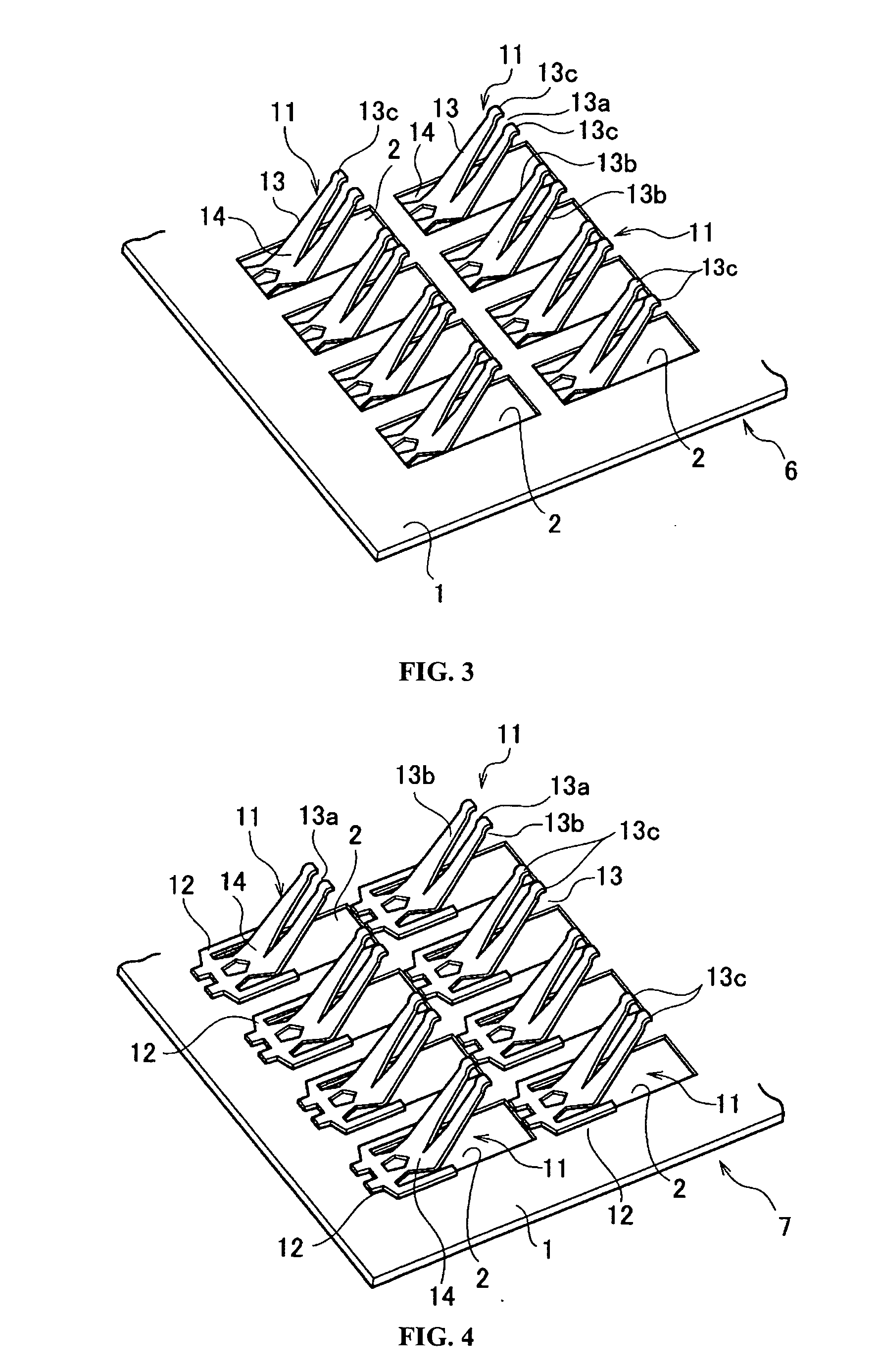
[0053] In FIGS. 1-6, the manufacturing process of a first embodiment of the present invention is shown. FIG. 1, FIGS. 2 and 3 and FIG. 4 respectively show the forming process of the base sheet, the forming process of the first bonded sheet, and the forming process of the second bonded sheet. FIG. 5 and FIG. 6 show a contact sheet and the bonding process for forming the contact sheet, respectively.

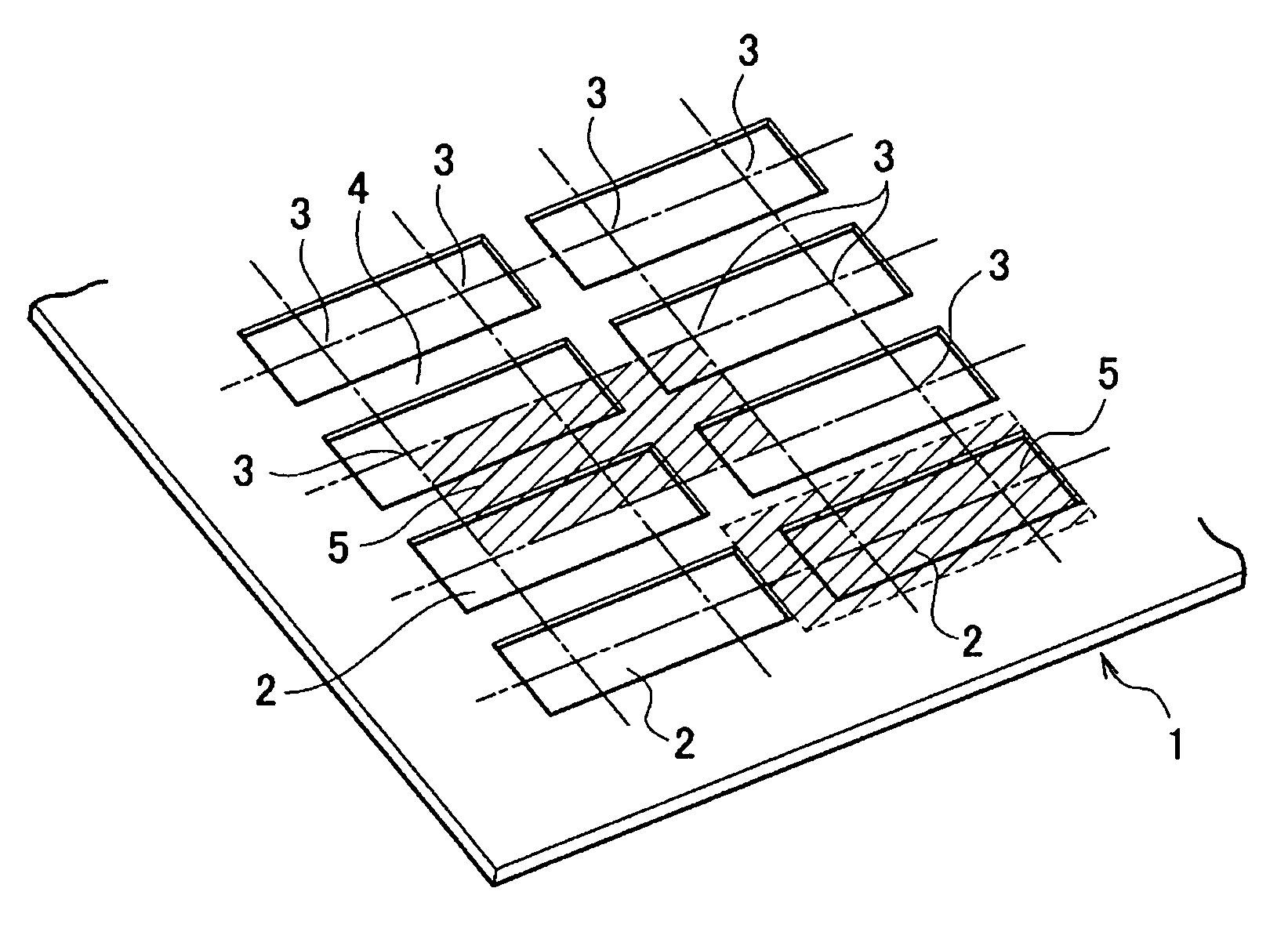
[0054] The base sheet 1 is made of a polyimide film. As shown in FIG. 1, the base sheet 1 has a plurality of through-holes 2 formed therein in an arrayed pattern. The square measure of the area of the through-hole 2 and the fixed part 12 of the contact 11 (see FIG. 4) is greater than the unit grid area formed by the arrangement of terminals (not shown) of the electronic device. That is, the amount of the square measure of the through-hole 2 and the fixed part 12 is configured to be larger than that of the unit grid area.

[0055] In FIG. 1, the reference number 3 indicates a center position ...

second embodiment

[0073]FIGS. 10-14 show a contact sheet in accordance with a second embodiment of this invention. In this embodiment, a through-hole 2 is formed in a base sheet 1 in a predetermined pattern and configured to correspond to a rectangle consisting of four contiguous unit grids which are formed by an arrangement of the terminals of an electronic device, which is shown as the hatched area 5 in FIG. 10. The through-hole 2 is formed by punching, laser cutting, etching with photosensitive film or any other suitable cutting method. An adhesive layer is formed on one side of the base sheet 1 by coating, either before or after forming the through-hole 2.

[0074] Meanwhile, a metal contact sheet consisting of a plurality of adjacent contacts connected to one another is produced by etching or punching a metal sheet as described above with respect to the first embodiment. In this metal contact sheet, a fixed part of the contact is configured so that the area overlapping the edge portion of the thro...

third embodiment

[0081]FIGS. 15-18 show a contact sheet in accordance with a third embodiment of the present invention.

[0082] In this embodiment, the through-hole 2 is configured as a square having a size that corresponds to a square consisting of four unit grids 4 which are formed by an arrangement of the terminals of an electronic device as shown in FIG. 15. Accordingly, the length of a side of the square through-hole 2 corresponds to twice the length of the side of the unit grid 4. Adopting such dimensions not only makes it easy to form the through-hole 2 but also enlarges the square measure width of a contact to be disposed therein and enables a corresponding increase in spring load.

[0083]FIG. 16 shows a base sheet 1 bonded with a metal contact sheet comprising a plurality of contacts 21. Each contact 21 comprises a fixed part (not shown) and a moving part including a second part 22 contiguous with the fixed part and a third contact portion 23 contiguous with the second part. The fixed part is...


PUM

PropertyMeasurementUnit
thicknessaaaaaaaaaa
thicknessaaaaaaaaaa
widthaaaaaaaaaa

Abstract

A contact sheet is provided including two insulative base sheets having a plurality of through-holes formed therethrough in an array pattern and a plurality of conductive contacts interposed between the insulative base sheets. Each contact includes a fixed part bonded to an end of a respective through-hole and an integral moving part contiguous with the fixed part. The moving part includes a contact portion formed as an elastic cantilever. Part of the moving part protrudes from one side of the base sheet inside the through-hole and the contact portion elastically extends from the other side of the base sheet. The total area of the through-hole and the fixed part of the contact is greater than a unit grid area formed by an arrangement of the terminals of an electronic device, and the length of the moving part, including the contact portion, substantially corresponds to the overall length of the through-hole.

Description

CROSS REFERENCE TO RELATED APPLICATIONS [0001] This application is a division of U.S. application Ser. No. 10 / 732,661, filed Dec. 10, 2003, and also claims the benefit of Japanese Application No. 2002-381617, filed Dec. 27, 2002, and Japanese Application No. 2003-361141, filed Oct. 21, 2003, the entireties of which are incorporated herein by reference.FIELD OF THE INVENTION [0002] The present invention relates to a contact sheet that is used for providing an electrical connection between electronic devices, such as integrated circuits, cables, and printed circuit boards, whose terminals are arranged on an edge part or in a grid pattern, methods of manufacturing such a contact sheet and a socket using the contact sheet. BACKGROUND OF THE INVENTION [0003] A contact sheet is put between electronic devices, such as integrated circuits, cables, and printed circuit boards, and is used to connect terminals of electric devices in order to shorten the length of electrical path and to reduce ...

Claims


Application Information

Patent Timeline
Patent Type & Authority Applications(United States)
IPC IPC(8): H01R9/28H01R12/16H01R13/24H01R33/76H01R12/04H01R43/00H01R43/16
CPCH01R9/28H01R13/2492H01R43/16Y10T29/49222Y10T29/4921Y10T29/49208Y10T29/49126Y10T29/49204H01R33/76
Inventor OCHIAI, TOSHIMASA
Owner NGK INSULATORS LTD
Why Eureka
Try Eureka