
Method and apparatus for electron-beam lithography
a technology of electron beam and electron beam, which is applied in the field of method and apparatus for electron beam lithography, can solve the problems of affecting the accuracy of the current stage, the factor of deterioration of the precision of the apparatus, and the disorder or degradation of the drawing precision, so as to achieve satisfactory drawing precision
- Summary
- Abstract
- Description
- Claims
- Application Information
AI Technical Summary
Benefits of technology
Problems solved by technology
Method used
Image

Examples
Embodiment Construction
[0026] Embodiments of the present invention will be described in conjunction with the drawings below.
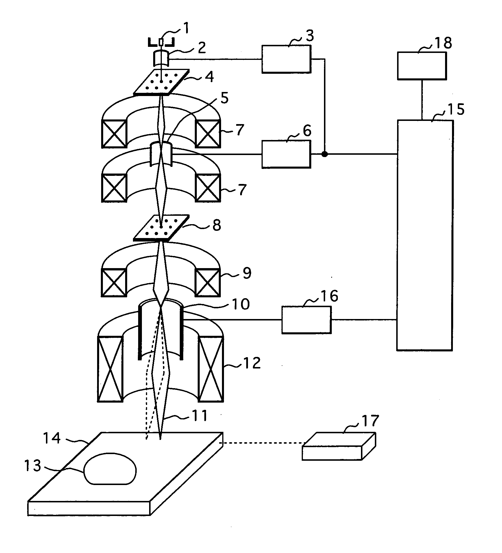
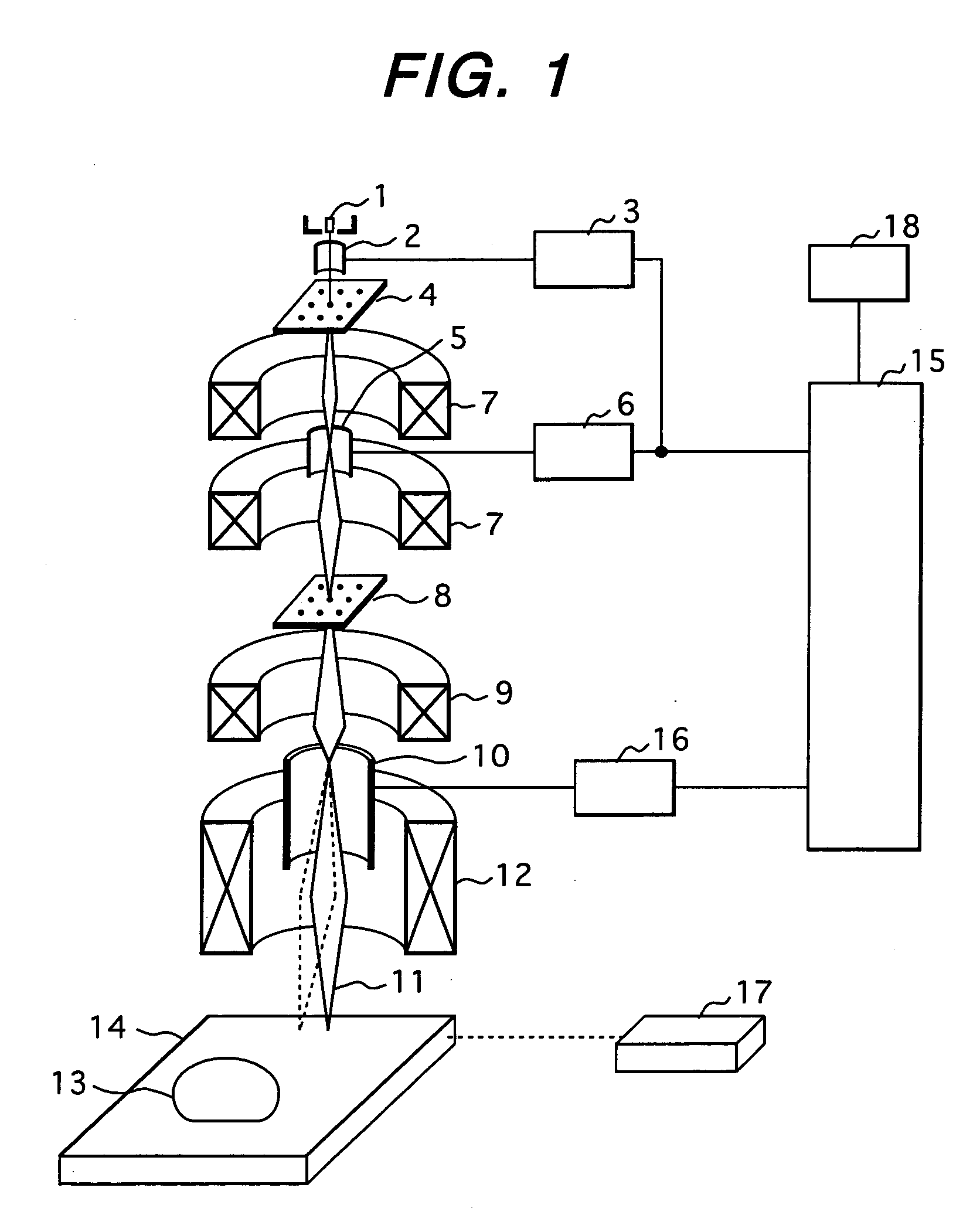
[0027] To begin with, an electron-beam lithography apparatus will be outlined below with reference to FIG. 1.
[0028] An electron beam 11 radiated from an electron source 1 is irradiated to a first mask 4 after being aligned by a beam aligner 2. A beam aligner control circuit 3 controls the beam aligner 2. The electron beam transmitted via the first mask 4 passes through a shaping lens 7 and reaches a second mask 8. When an electron beam is irradiated to the second mask8, a control computer 15 instructs a shaping deflection control circuit 6 to determine a dimension for the electron beam-shape. The shaping deflection control circuit 6 applies a voltage on the determined dimension to the shaping deflector 5, whereby a rectangular electron beam is transmitted by the second mask 8 so that it will have the determined dimension on a wafer 13.
[0029] The shaping deflector 5 and shaping def...
PUM
 Abstract
Description
Claims
Application Information