Output buffer with selectable slew rate

a buffer and selectable technology, applied in the direction of pulse manipulation, logic circuit coupling/interface arrangement, pulse technique, etc., can solve the problems of circuitry being extremely fast, prone to external voltage and current, and exceeding the ability of internal circuits, etc., to achieve the effect of fast slew ra

Inactive Publication Date: 2006-01-19
AVAGO TECH INT SALES PTE LTD
View PDF7 Cites 6 Cited by
  • Summary
  • Abstract
  • Description
  • Claims
  • Application Information

AI Technical Summary

Problems solved by technology

While direct electrical connection with internal components of an IC is possible, it would leave the IC vulnerable to external voltages and currents, which may exceed the ability of the internal circuit.
In particular, while internal circuitry may be extremely fast operating, a buffer may be slower because of its relatively larger size to provide suitable protection as well as drive a suitable level of output current.
Slew rate causes distortion for high frequency large signal operation.
High slew rates are good from a signal standpoint as it means that the output of a buffer very quickly follows the input signal to that buffer, but it comes at the price of increased transient noise in the system.
The downside of high speed operation with such a buffer is that higher slew rates necessary to achieve such high speed operation will cause more electrical noise such as transient noise in the integrated circuit.
Such noise is often carried through many parts of the IC, e.g., through a power and / or ground rail.
Because of the 4-fold area expense for portions of the buffer due to adding slew rate control to a buffer, the design of conventional buffers requires an area appreciably larger than that of buffers that do not have this feature.

Method used


Image

  • Output buffer with selectable slew rate
  • Output buffer with selectable slew rate
  • Output buffer with selectable slew rate

Examples


Embodiment Construction

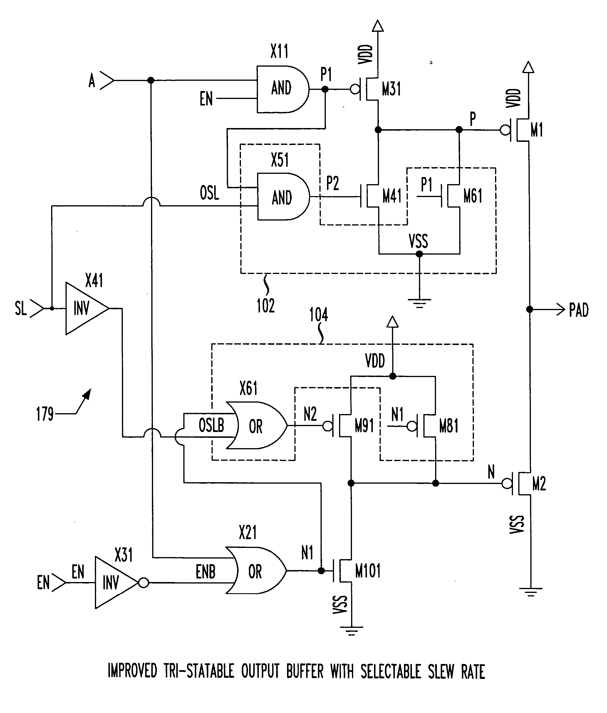
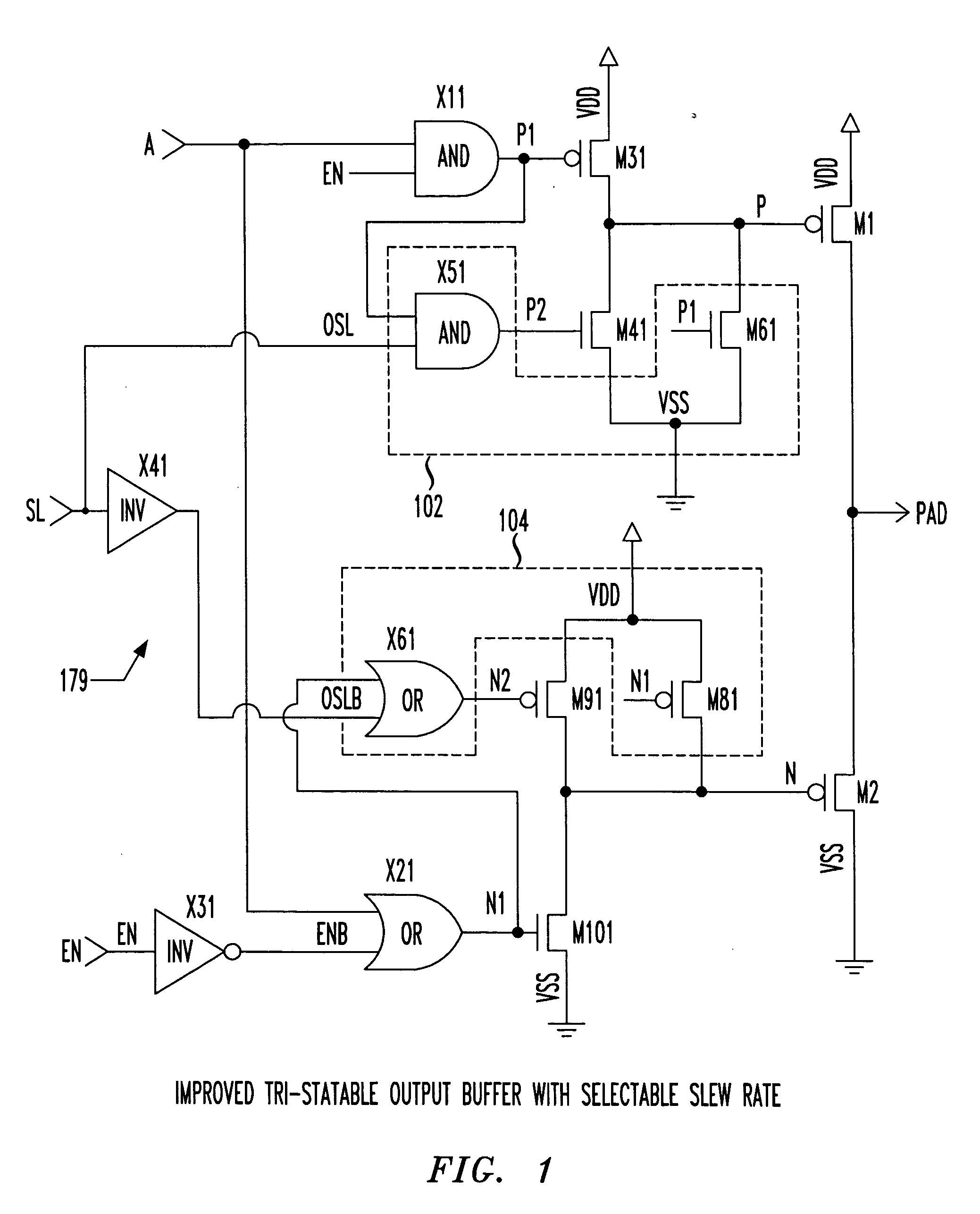
[0037] The present invention provides a buffer design for an integrated circuit that has adjustable slew rate control, yet requires significantly less space to fabricate than does a conventional buffer with slew rate control.

[0038] In accordance with the principles of the present invention, a new slew rate control circuit design is added to a Complementary Metal Oxide Semiconductor CMOS buffer to implement slew rate control in the buffer (e.g., selection between a high slew rate and a low slew rate). The new slew rate control circuit requires significantly less space to fabricate, and when applied to each buffer in an given integrated circuit, e.g., input / output buffers that may be placed along the periphery of the integrated circuit, the savings can be extraordinary.

[0039]FIG. 1 shows an improved circuit including a new slew rate control circuit 179 that includes all of the advantages provided by an adjustable slew rate buffer—without the large area penalty associated with conven...


PUM


Abstract

A buffer design for an integrated circuit that has adjustable slew rate control, yet requires significantly less space to fabricate than does a conventional buffer with slew rate control. A new slew rate control circuit design is added to a Complementary Metal Oxide Semiconductor CMOS buffer to implement slew rate control in the buffer (e.g., selection between a high slew rate and a low slew rate). The new slew rate control circuit requires significantly less space to fabricate, and when applied to each buffer in an given integrated circuit, e.g., input / output buffers that may be placed along the periphery of the integrated circuit, the savings can be extraordinary.

Description

BACKGROUND OF THE INVENTION [0001] 1. Field of the Invention [0002] This invention relates to the design of integrated circuits. More particularly, it relates to the design of input and output buffers in an integrated circuit. [0003] 2. Background of Related Art [0004] Integrated circuits are an important part of life as we know it today. They are the basis for most all electronic device, from telephones and answering machines to the most sophisticated computers. An important part of an integrated circuit (IC) is its ability to accept information in, and / or to pass information out. Thus, an IC must interface with the outside world. [0005] While direct electrical connection with internal components of an IC is possible, it would leave the IC vulnerable to external voltages and currents, which may exceed the ability of the internal circuit. To provide both protection of internal components from external signals, as well as to provide amplified output signals, most signals input or out...

Claims


Application Information

Patent Timeline
Patent Type & Authority Applications(United States)
IPC IPC(8): H03B1/00
CPCH03K17/163
Inventor HUBER, CAROL ANNKRIZ, JOHN C.LACEY, BRIAN C.MORRIS, BERNARD L.
Owner AVAGO TECH INT SALES PTE LTD
Why Eureka
Try Eureka