RFID tag, RFID-tag antenna, RFID-tag antenna sheet, and method of manufacturing RFID tag

a technology of rfid tag and antenna, which is applied in the direction of antenna details, instruments, antennas, etc., can solve the problems of increasing the length of the antenna, increasing the weight of the film base, and limiting the improvement of the reception sensitivity of polarized waves and directivity of the plane antenna

Inactive Publication Date: 2006-03-02
FUJITSU LTD
View PDF10 Cites 119 Cited by
  • Summary
  • Abstract
  • Description
  • Claims
  • Application Information

AI Technical Summary

Benefits of technology

[0020] It is an object of the present invention to solve at least the above problems in the conventional technology.
[0021] A radio-frequency-identification tag antenna according to one aspect of the present invention includes a film base; a plurality of antenna patterns for transmission and reception, the antenna patterns being formed in parallel on the film base; and a cut line that is formed on the film base between adjacent antenna patterns along the antenna patterns from an inside to an outer edge of the film base. A part of the film base on which the antenna patterns are formed is folded or bent in a predetermined direction using the cut line.
[0022] A radio-frequency-identification tag according to another aspect of the present invention includes a film base; a plurality of antenna patterns for transmission and reception, the antenna patterns being formed in parallel on the film base; a cut line that is formed on the film base between adjacent antenna patterns along the antenna patterns from an inside to an outer edge of the film base; and an integrated-circuit chip that incorporates a communication circuit and a memory circuit, the integrated-circuit chip being electrically connected to the antenna patterns. A part of the film base on which the antenna patterns are formed is folded or bent in a predetermined direction using the cut line.
[0023] An radio-frequency-identification tag antenna sheet according to still another aspect of the present invention is formed as a group of the radio-frequency-identification tag antennas, on which a plurality of a radio-frequency-identification tag antennas is disposed on a same plane. The radio-frequency-identification tag antenna includes a film base; a plurality of antenna patterns for transmission and reception, the antenna patterns being formed in parallel on the film base; and a cut line that is formed on the film base between adjacent antenna patterns along the antenna patterns from an inside to an outer edge of the film base. A part of the film base on which the antenna patterns are formed is folded or bent in a predetermined direction using the cut line.
[0024] A method of manufacturing a radio-frequency-identification tag according to still another aspect of the present invention includes forming a plurality of antenna patterns for transmission and reception in parallel on a film base; connecting electrically an integrated-circuit chip that incorporates a communication circuit and a memory circuit, onto each of the antenna patterns; forming a cut line on the film base between adjacent antenna patterns along the antenna patterns from an inside to an outer edge of the film base; and forming a desired shape of an antenna by folding or bending the film base formed with the antenna patterns in a predetermined direction by using the cut line.

Problems solved by technology

In addition, the plane antenna has a limit in improvement of reception sensitivity of a polarized wave and in directivity.
Moreover, a communication distance cannot be increased.
Therefore, when this material is used to form a three-dimensional antenna, an increased length of the antenna increases a weight of the film base.
As a result, the film base can hardly maintain a shape without flexure.
Consequently, the performance the antenna is degraded.
Although stiffness of the antenna increases because of the reinforcement, manufacturing cost increases by an increase process.
However, since the antenna is a plane coil antenna, there is a limit to the improvement in the reception sensitivity of a polarized wave or the improvement in directivity.
Further, a communication distance cannot be increased.

Method used


Image

  • RFID tag, RFID-tag antenna, RFID-tag antenna sheet, and method of manufacturing RFID tag
  • RFID tag, RFID-tag antenna, RFID-tag antenna sheet, and method of manufacturing RFID tag
  • RFID tag, RFID-tag antenna, RFID-tag antenna sheet, and method of manufacturing RFID tag

Examples


first embodiment

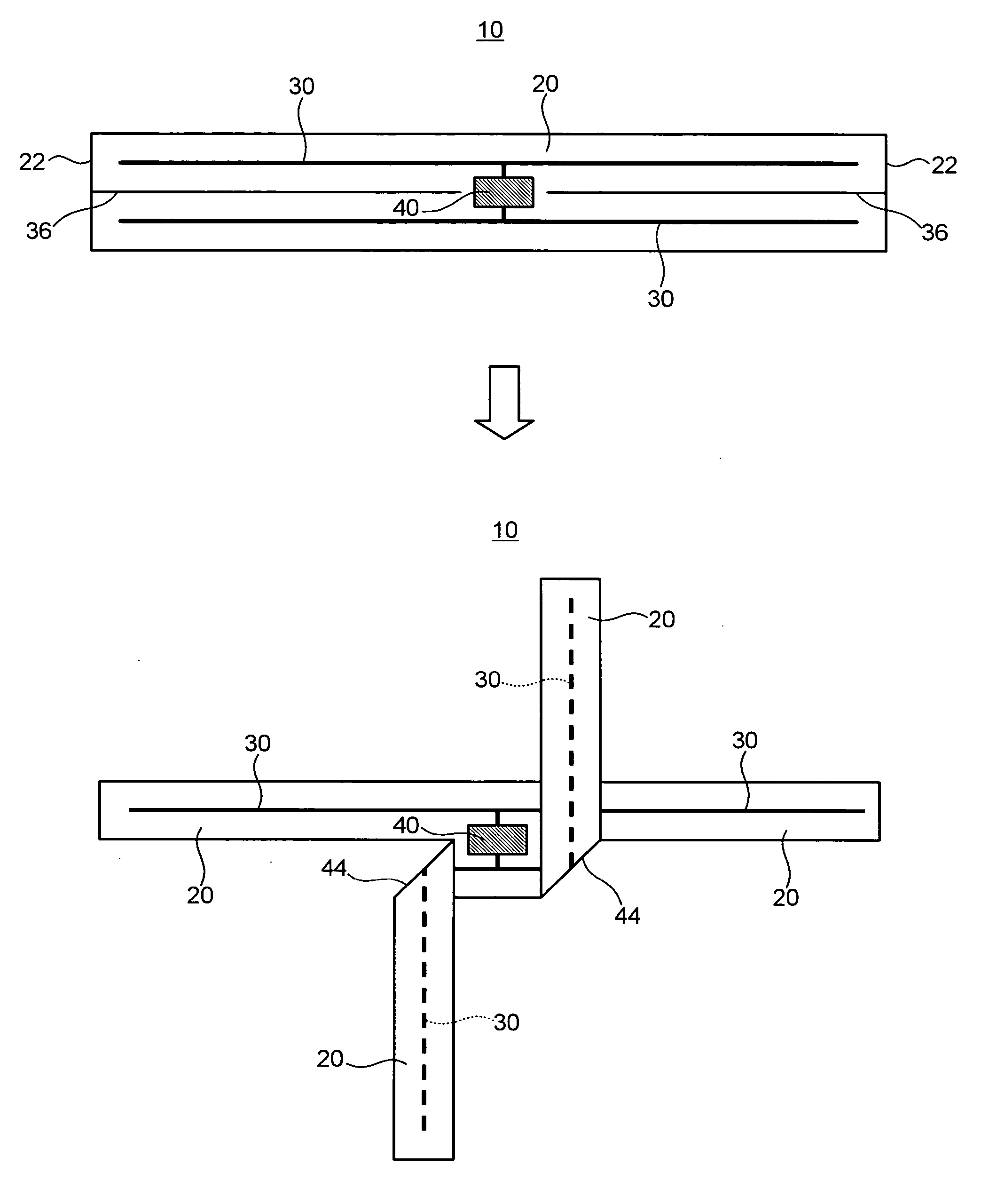
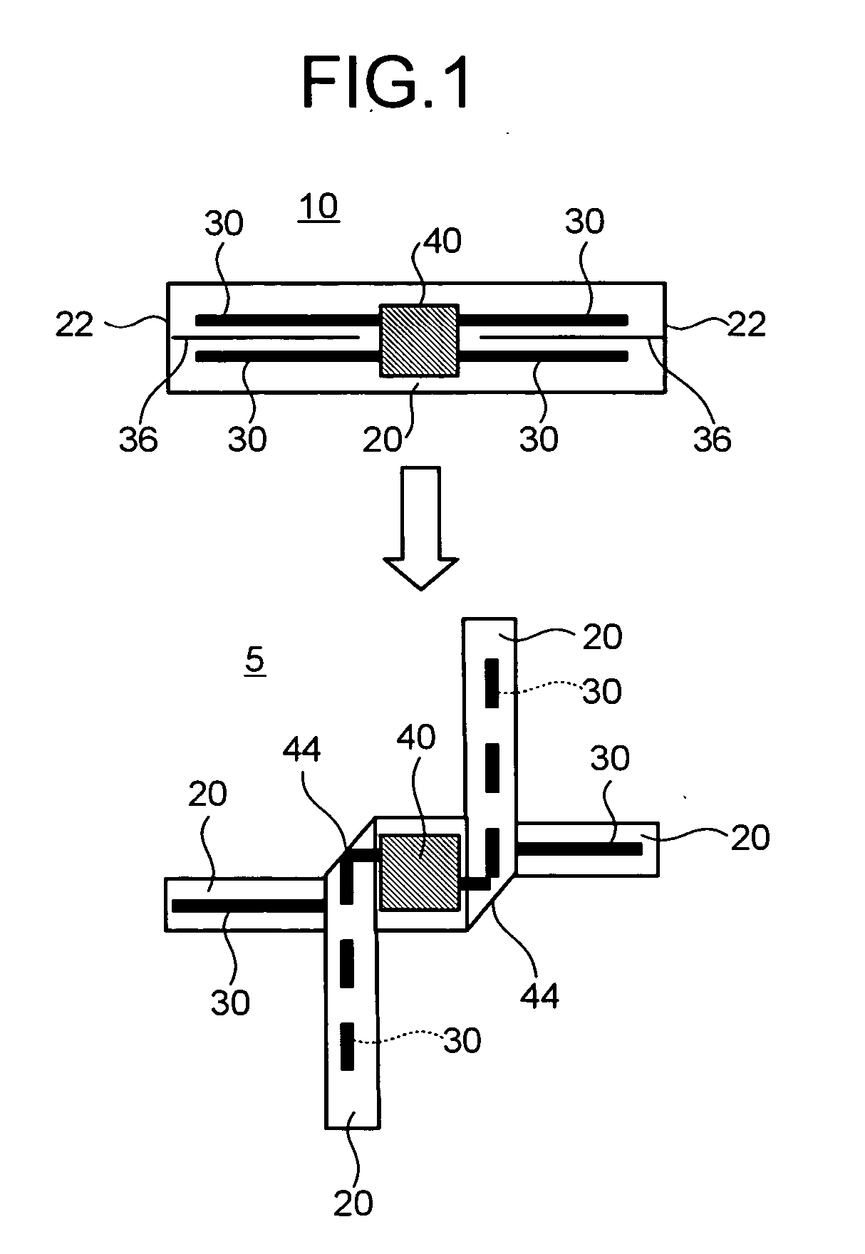
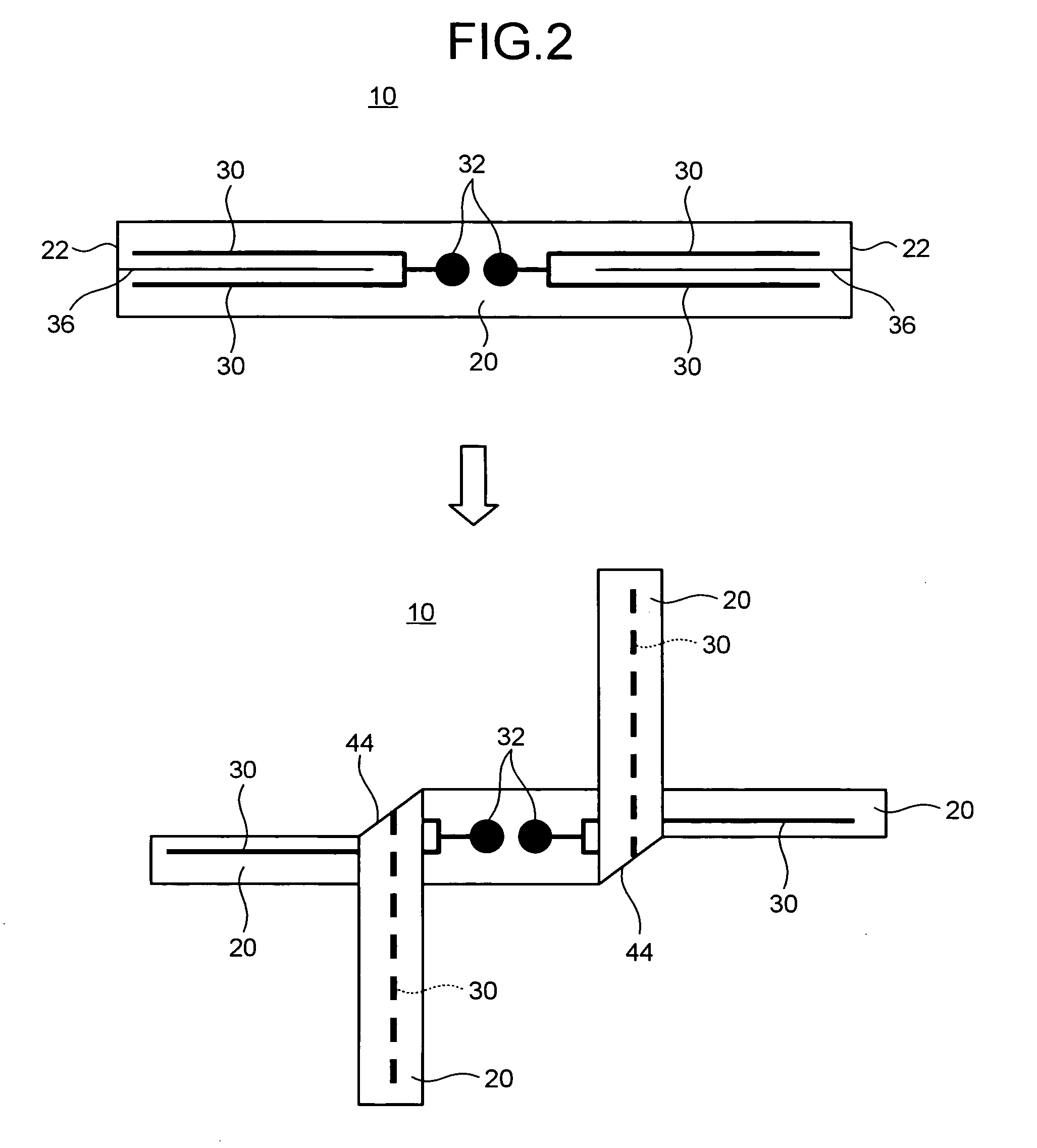
[0051]FIG. 1 is a top plan view of an RFID tag according to the present invention, illustrating a process of forming the RFID tag. FIG. 2 is a top plan view of an RFID tag antenna, illustrating a process of folding the antenna. FIG. 3 is a top plan view of an RFID-tag antenna sheet.

[0052] As shown in FIG. 1, an RFID tag antenna 10 that forms an RFID tag 5 includes a film base 20, transmission / reception antenna patterns 30 that are formed in two rows in parallel on the film base 20, a cut line 36 formed on the film base 20 between the adjacent antenna patterns 30 along the antenna patterns 30 from the inside of the film base 20 to reach an external edge 22, and an IC chip 40 that is electrically connected to the antenna patterns 30.

[0053] In the present specification, the film base 20 with the IC chip 40 mounted thereon and that without mounting the IC chip 40 are both called an “RFID tag antenna”.

[0054] The film base 20 is made of flexible thermoplastics. In other words, PET, poly...

second embodiment

[0072]FIG. 4 is a top plan view of an RFID tag according to the present invention, illustrating a process of forming the RFID tag. FIG. 5 is a perspective view of the RFID tag. FIG. 6 is a perspective view of an RFID tag that is incorporated in a golf ball. In the explanation below, like reference numerals designate like or similar parts as those already explained and a redundant explanation is omitted.

[0073] An RFID tag antenna 10 according to the second embodiment is different from that according to the first embodiment in the following points. As shown in FIG. 4 and FIG. 5, the RFID tag antenna 10 includes the transmission / reception antenna patterns 30 that are formed in three parallel rows on the film base 20, and the cut lines 36 that are formed on the film base 20 between the adjacent antenna patterns 30 along the antenna patterns 30 from the inside of the film base 20 to reach the external edge 22. The three-row antenna patterns 30 formed on the film base 20 are folded in a p...

eighth embodiment

[0094] A main difference is that RFID tag antenna 10 has adhesive pads 34a and 34b, which are coated with conductive adhesive exhibiting a predetermined adhesive force by pressing and heating, formed at the ends of the antenna patterns 30.

[0095] As shown in FIG. 12 and FIG. 13, a set of film bases 20 are folded at the folding sections 44 using the cut lines 36, and at the same time, another set of film bases 20 are also bent. The adhesive pads 34a and 34a are adhered together, and the adhesive pads 34b and 34b are adhered together, on the film bases 20 respectively.

[0096] By bonding the ends of the film base 20 together, one loop antenna 38 is formed above the IC chip 40, and another loop antenna 38 is formed below the IC chip 40. In FIG. 13, a state after the adhesion between the adhesive pads 34a and 34a is shown using an imaginary line.

[0097] As explained above, according to the eighth embodiment, the RFID tag 5 can secure a sufficiently high production yield from the material...


PUM


Abstract

A radio-frequency-identification tag antenna includes a film base, a plurality of antenna patterns for transmission and reception, which is formed in parallel on the film base, and a cut line that is formed on the film base between adjacent antenna patterns along the antenna patterns from an inside to an outer edge of the film base. A part of the film base on which the antenna patterns are formed is folded or bent in a predetermined direction using the cut line.

Description

BACKGROUND OF THE INVENTION [0001] 1) Field of the Invention [0002] The present invention relates to a radio frequency identification (RFID) tag, an RFID-tag antenna, an RFID tag antenna sheet for a non-contact IC card that receives power and information from an external device and transmits information to the external device, and a method of manufacturing the RFID tag. [0003] 2) Description of the Related Art [0004] Recently, an RFID tag (also referred to as an RFID-tag inlay, a radio IC tag, a non-contact IC tag, etc) for a non-contact integrated-circuit (IC) card that receives power and information from an external device such as a reader / writer and transmits information to the external device, without making a contact using a radio wave became popular. FIG. 18 is a plan view of a conventional RFID tag. As shown in FIG. 18, for example, an RFID tag 100 includes an antenna pattern 102 and an IC chip 103 that are provided on a film base 101 formed with a material such as plastics. ...

Claims


Application Information

Patent Timeline
Patent Type & Authority Applications(United States)
IPC IPC(8): G06K19/06
CPCA63B43/00A63B2225/54G06K19/07749H01Q7/00G06K19/07786H01Q1/2208G06K19/07758G06K19/077
Inventor BABA, SHUNJIISHIKAWA, NAOKIKOBAYASHI, HIROSHIYAMAKAMI, TAKATOYOKATAYAMA, MASUMI
Owner FUJITSU LTD
Why Eureka
Try Eureka