Chip structure
a technology of semiconductor chips and chips, applied in the direction of semiconductor devices, semiconductor/solid-state device details, electrical apparatus, etc., can solve the problem that the bump is unsuitable for being processed using a reflow process, and achieve the effect of maximizing the use of space over the passivation layer
- Summary
- Abstract
- Description
- Claims
- Application Information
AI Technical Summary
Benefits of technology
Problems solved by technology
Method used
Image

Examples
first embodiment
[0033] In the first embodiment, the metal circuit layer is placed over the passivation layer and the bump is placed over the metal circuit layer. This embodiment has several applications, as is illustrated in the following.
[0034] 1. Application to Intra-Chip Signal Transmission
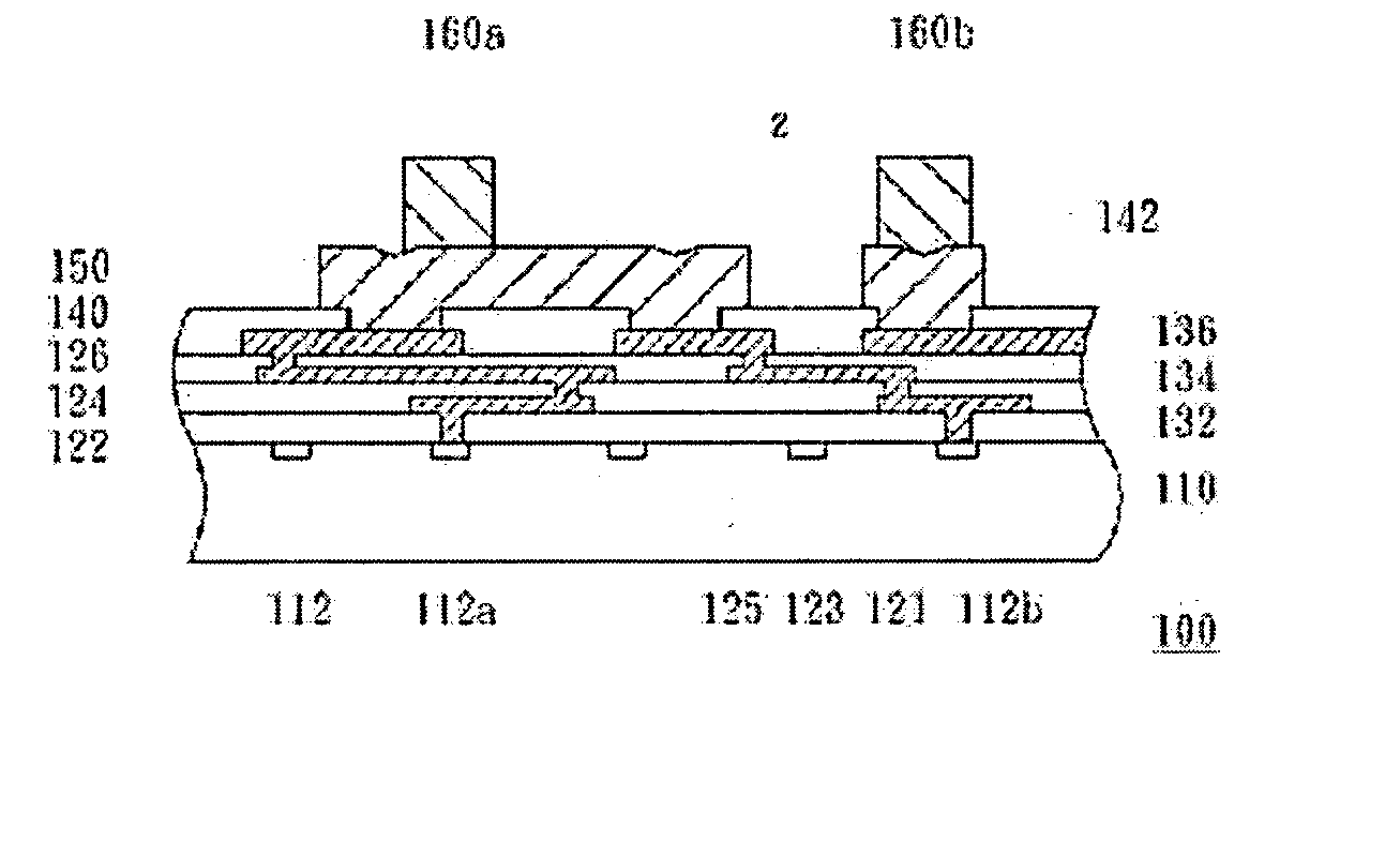
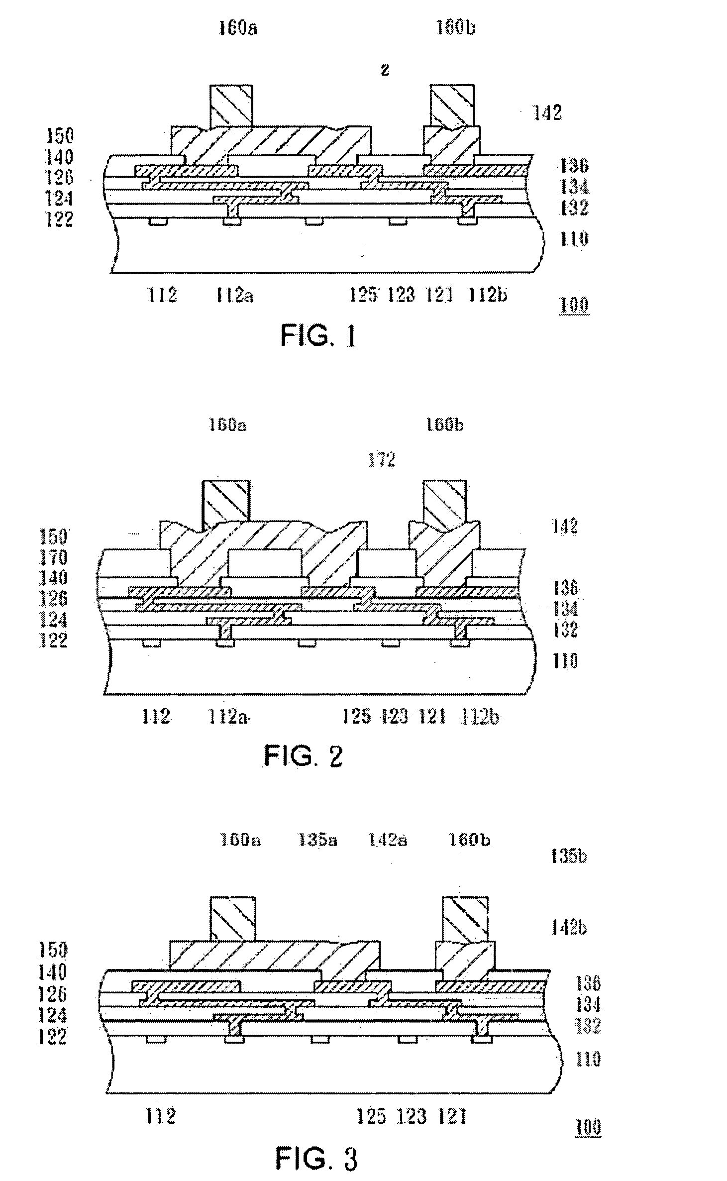
[0035]FIGS. 1-2 are schematic cross-sectional figure showing the chip structures or wafer structures according to a first embodiment of the present invention. The metal circuit layer 150, for example, is used for intra-chip signal transmission. The chip structure or wafer structure 100 comprises a semiconductor substrate 110, a plurality of thin film dielectric layers 122, 124 and 126, a plurality of thin film fine line metal layers 132, 134 and 136, and a passivation layer 140. The chip structure is obtained after sawing the wafer structure.
[0036] The semiconductor substrate 110 comprises a plurality of electronic devices 112 formed in or on the semiconductor substrate 110. The semiconductor substrate 110,...
second embodiment
[0058] In the second embodiment, the metal circuit 250 is positioned over the passivation layer 140 and the bump 260 is positioned on the topmost thin film fine line metal layer 136. The components below the passivation layer 140 of the chip structure 200 in the second embodiment are similar to the above-mentioned in FIGS. 1-2.
[0059] This embodiment has several applications, as illustrated in the following.
[0060] 1. Application to Intra-Chip Signal Transmission
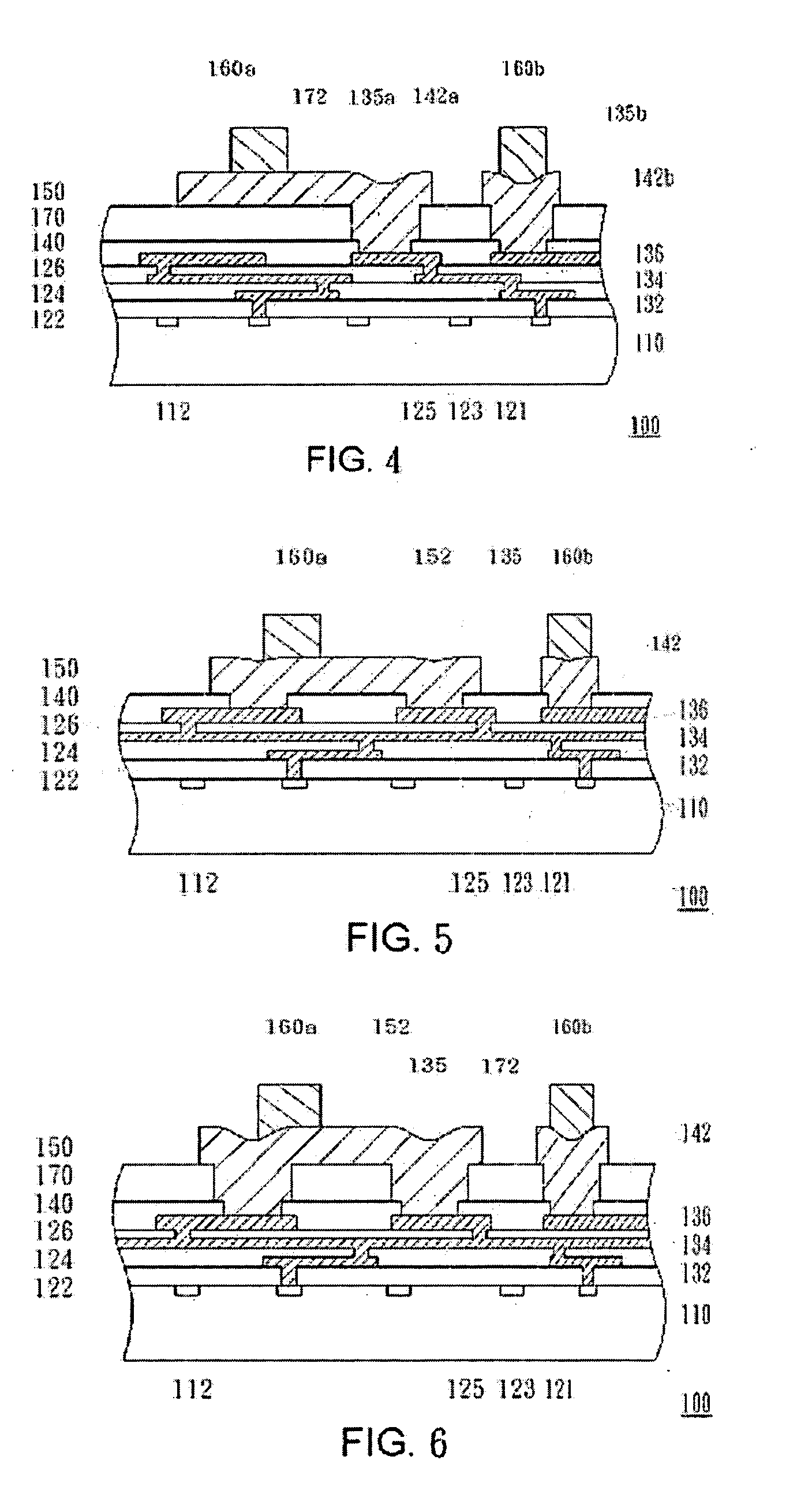
[0061]FIGS. 11-23 are schematic cross-sectional figures showing the chip structures according to a second embodiment of the present invention. A circuit line at the left side of the metal circuit layer 250 is used for intra-chip signal transmission.
[0062] In FIGS. 11-23, a metal circuit layer 250 is formed over the passivation layer 140 and electrically connected to the thin film fine line metal layer 136 through openings 142 in the passivation layer 140. The metal circuit 250 connects multiple pads of the thin film fine l...
PUM
 Abstract
Description
Claims
Application Information
 - R&D
- Intellectual Property
- Life Sciences
- Materials
- Tech Scout
- Unparalleled Data Quality
- Higher Quality Content
- 60% Fewer Hallucinations
Browse by: Latest US Patents, China's latest patents, Technical Efficacy Thesaurus, Application Domain, Technology Topic, Popular Technical Reports.
© 2025 PatSnap. All rights reserved.Legal|Privacy policy|Modern Slavery Act Transparency Statement|Sitemap|About US| Contact US: help@patsnap.com