Microelectronic imagers with optical devices and methods of manufacturing such microelectronic imagers

a microelectronic imager and optical device technology, applied in the field of microelectronic imagers and methods for packaging microelectronic imagers, can solve the problems of time-consuming and labor-intensive positioning of the lens at the desired focus distance from the image sensor, and the difficulty of accurately aligning the lens with the image sensor

Active Publication Date: 2006-11-02
APTINA IMAGING CORP
View PDF87 Cites 187 Cited by
  • Summary
  • Abstract
  • Description
  • Claims
  • Application Information

AI Technical Summary

Problems solved by technology

One problem with packaging conventional microelectronic imagers is that it is difficult to accurately align the lens with the image sensor.
This is difficult to achieve with conventional imagers because the support 50 may not be positioned accurately on the housing 30, and the barrel 60 is manually threaded onto the support 50.
Another problem of packaging conventional microelectronic imagers is that positioning the lens at a desired focus distance from the image sensor is time-consuming and may be inaccurate.
This process is problematic because it is exceptionally time-consuming, subject to operator errors, and subject to axial misalignment between the support 50 and the barrel 60.
Yet another concern of conventional microelectronic imagers is that they have relatively large footprints and occupy a significant amount of vertical space (i.e., high profiles).
This is typically much larger than the surface area of the die 10 and can be a limiting factor in the design and marketability of picture cell phones or PDAs because these devices are continually shrinking to be more portable.
Yet another concern of conventional microelectronic imagers is the manufacturing costs for packaging the dies.
The imager 1 shown in FIG. 1 is relatively expensive because manually adjusting the lens 70 relative to the image sensor 12 is very inefficient and subject to error.

Method used


Image

  • Microelectronic imagers with optical devices and methods of manufacturing such microelectronic imagers
  • Microelectronic imagers with optical devices and methods of manufacturing such microelectronic imagers
  • Microelectronic imagers with optical devices and methods of manufacturing such microelectronic imagers

Examples


Embodiment Construction

A. Overview

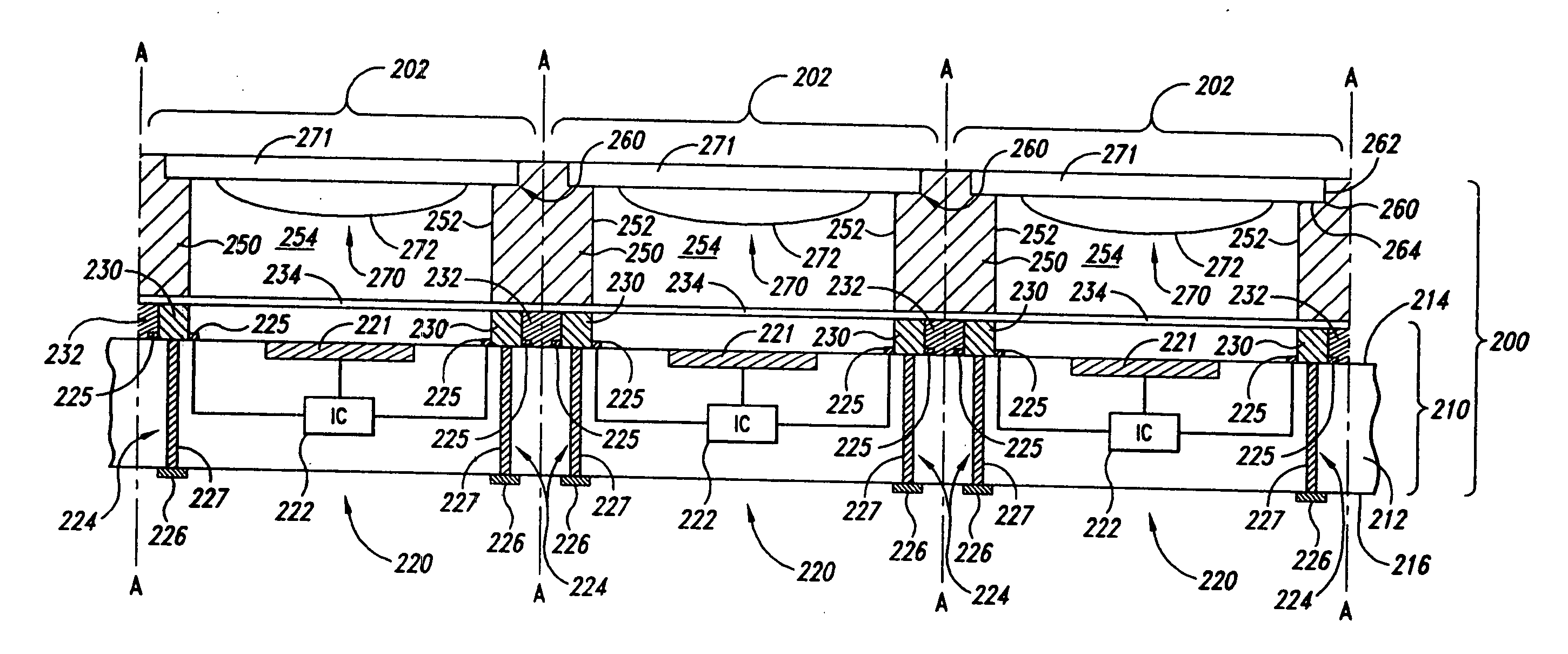
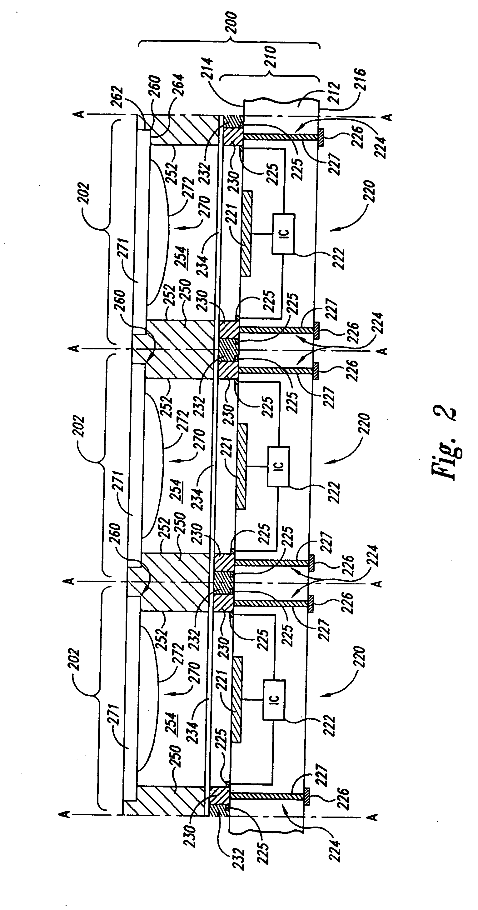
[0018] The following disclosure describes several embodiments of methods for assembling optical devices with microelectronic imaging units and microelectronic imagers that are formed using such methods. One aspect of the invention is directed toward methods of manufacturing microelectronic imagers. An embodiment of one such method comprises providing an imager workpiece and constructing optics supports on the imager workpiece. The imager workpiece has a plurality of imaging dies that include image sensors and external contacts operatively coupled to the image sensors. The imaging dies can be on and / or in a first substrate such that the image sensors are at a front side of the first substrate. The optics supports are constructed on the imager workpiece before cutting the imager workpiece. The optics supports, for example, can be constructed on the first substrate or on a cover attached to the first substrate. The optics supports include openings aligned with corresponding ...


PUM


Abstract

Microelectronic imager assemblies comprising a workpiece including a substrate and a plurality of imaging dies on and/or in the substrate. The substrate includes a front side and a back side, and the imaging dies comprise imaging sensors at the front side of the substrate and external contacts operatively coupled to the image sensors. The microelectronic imager assembly further comprises optics supports superimposed relative to the imaging dies. The optics supports can be directly on the substrate or on a cover over the substrate. Individual optics supports can have (a) an opening aligned with one of the image sensors, and (b) a bearing element at a reference distance from the image sensor. The microelectronic imager assembly can further include optical devices mounted or otherwise carried by the optics supports.

Description

TECHNICAL FIELD [0001] The present invention is related to microelectronic imagers and methods for packaging microelectronic imagers. Several aspects of the present invention, more specifically, are directed toward installing optical devices in microelectronic imagers. BACKGROUND [0002] Microelectronic imagers are used in digital cameras, wireless devices with picture capabilities, and many other applications. Cell phones and Personal Digital Assistants (PDAs), for example, are incorporating microelectronic imagers for capturing and sending pictures. The growth rate of microelectronic imagers has been steadily increasing as they become smaller and produce better images with higher pixel counts. [0003] Microelectronic imagers include image sensors that use Charged Coupled Device (CCD) systems, Complementary Metal-Oxide Semiconductor (CMOS) systems, or other systems. CCD image sensors have been widely used in digital cameras and other applications. CMOS image sensors are also quickly ...

Claims


Application Information

Patent Timeline
Patent Type & Authority Applications(United States)
IPC IPC(8): H01L27/00
CPCH01L27/14618H01L27/14625H01L27/14683H01L27/14687H01L2224/48091H01L2924/01078H01L2224/48227H01L2924/01077H01L2924/00014B33Y80/00H01L27/00
Inventor FARNWORTH, WARREN M.RIGG, SIDNEY B.HIATT, WILLIAM MARKWOOD, ALAN G.BENSON, PETER A.WARK, JAMES M.HEMBREE, DAVID R.KIRBY, KYLE K.WATKINS, CHARLES M.AKRAM, SALMAN
Owner APTINA IMAGING CORP
Why Eureka
Try Eureka