Method and structure for reducing the external resistance of a three-dimensional transistor through use of epitaxial layers

a three-dimensional transistor and epitaxial layer technology, applied in the field of semiconductor processing of transistors, can solve the problems of limited cross-sectional area, high external resistance, and high external resistan

Inactive Publication Date: 2007-07-05
INTEL CORP
View PDF99 Cites 29 Cited by
  • Summary
  • Abstract
  • Description
  • Claims
  • Application Information

AI Technical Summary

Problems solved by technology

One problem with some of these devices is the generally high external resistance that comes about from the thinning of the source and drain regions, sometimes at the edge

Method used


Image

  • Method and structure for reducing the external resistance of a three-dimensional transistor through use of epitaxial layers
  • Method and structure for reducing the external resistance of a three-dimensional transistor through use of epitaxial layers
  • Method and structure for reducing the external resistance of a three-dimensional transistor through use of epitaxial layers

Examples


Embodiment Construction

[0012] A process for fabricating CMOS field-effect transistors and the resultant transistors are described. In the following description, numerous specific details are set forth, such as specific dimensions and chemical regimes, in order to provide a thorough understanding of the present invention. It will be apparent to one skilled in the art that the present invention may be practiced without these specific details. In other instances, well-known processing steps, such as cleaning steps, are not described in detail, in order to not unnecessarily obscure the present invention.

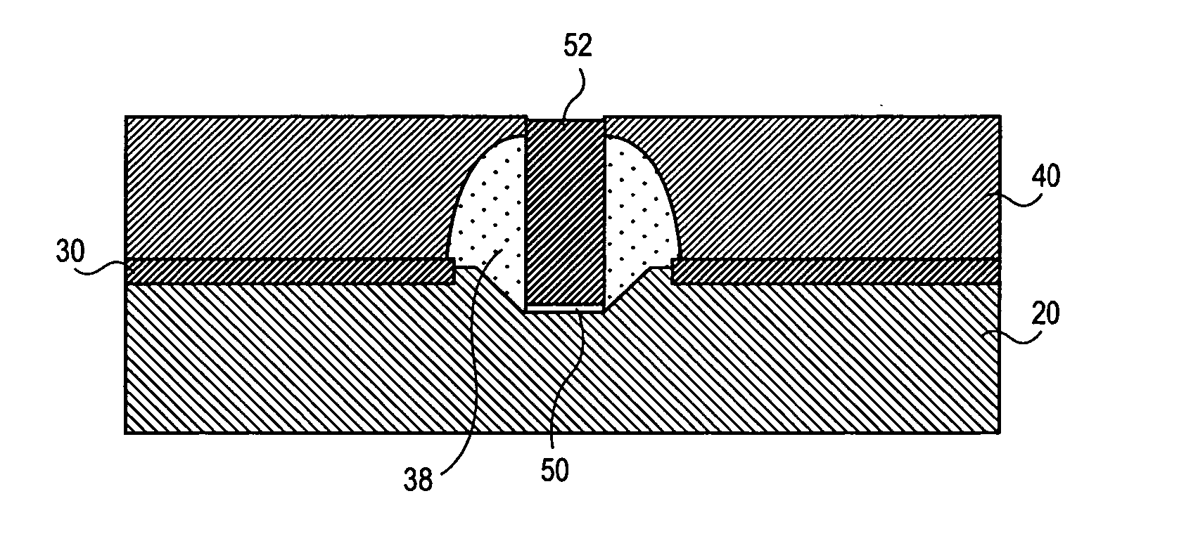
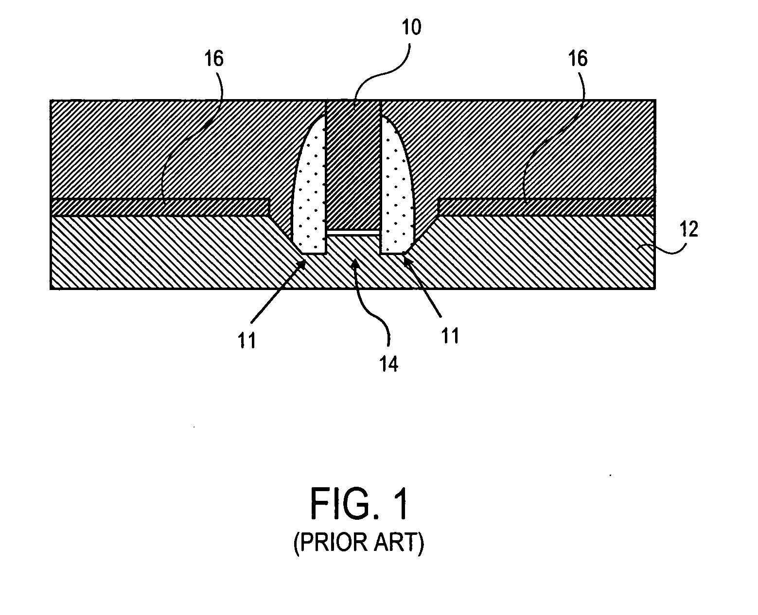
[0013] A problem associated with small body transistors is illustrated in FIG. 1. A gate structure 10 is shown traversing a semiconductor body 12 at a channel region 14 of a transistor having source / drain regions 16. The semiconductor body or fin is thinned at the gate edges 11. This thinning is the result of processing used for defining the body, forming spacers, and cleaning of oxides. This processing can r...


PUM


Abstract

The fabrication of a tri-gate transistor formed with a replacement gate process is described. A nitride dummy gate, in one embodiment, is used allowing the growth of epitaxial source and drain regions immediately adjacent to the dummy gate. This reduces the external resistance.

Description

FIELD OF THE INVENTION [0001] The invention relates to the field of semiconductor processing for transistors having thin channel regions. PRIOR ART AND RELATED ART [0002] The trend in the fabrication of complementary metal-oxide-semiconductor (CMOS) transistors is to have small channel regions. Examples of a transistor having a reduced body which includes the channel region along with a tri-gate structure are shown in US 2004 / 0036127. Other small channel transistors are delta-doped transistors formed in lightly doped or undoped epitaxial layers grown on a heavily doped substrate. See, for instance, “Metal Gate Transistor with Epitaxial Source and Drain Regions,” application Ser. No. 10 / 955,669, filed Sep. 29,2004, assigned to the assignee of the present application. [0003] One problem with some of these devices is the generally high external resistance that comes about from the thinning of the source and drain regions, sometimes at the edges of the gates. Other devices have similar ...

Claims


Application Information

Patent Timeline
IPC IPC(8): H01L29/76
CPCH01L29/66545H01L29/66628H01L29/785H01L29/7848H01L29/66795
Inventor DOYLE, BRIAN S.BRASK, JUSTIN K.MAJUMDAR, AMLANDATTA, SUMANKAVALIEROS, JACKRADOSAVLJEVIC, MARKOCHAU, ROBERT S.
Owner INTEL CORP
Why Eureka
Try Eureka