3-d package stacking system

a technology of stacking system and 3d package, which is applied in the direction of solid-state devices, basic electric elements, electrical apparatus construction details, etc., can solve the problems of inefficiency of kgd, difficult to test the die before assembly on the substrate, and the vertical or horizontal arrangement of multi-chip modules

Active Publication Date: 2007-08-16
STATS CHIPPAC LTD
View PDF28 Cites 91 Cited by
  • Summary
  • Abstract
  • Description
  • Claims
  • Application Information

AI Technical Summary

Problems solved by technology

However, multi-chip modules, whether vertically or horizontally arranged, can also present problems because they usually must be assembled before the component chips and chip connections can be tested.
That is, because the electrical bond pads on a die are so small, it is difficult to test die before assembly onto a substrate.
With conventional multi-chip modules, however, the die cannot be individually identified as KGD before final assembly, leading to KGD inefficiencies and assembly process yield problems.
As discussed, both these methods have inherent KGD and assembly process yield loss disadvantages since KGD cannot be used for fabricating these configurations.
But package level stacking can pose other problems.
One problem is package-to-package assembly process difficulties caused by irregularities in the flatness / coplanarity of the lower package.
Another problem results from the increased stiffness of the overall assembly, which can lead to reduced board level reliability.
Still another problem can arise from poor heat dissipation from the upper package.
Solutions to these problems have been long sought but prior developments have not taught or suggested any solutions and, thus, solutions to these problems have long eluded those skilled in the art.

Method used


Image

  • 3-d package stacking system
  • 3-d package stacking system
  • 3-d package stacking system

Examples


Embodiment Construction

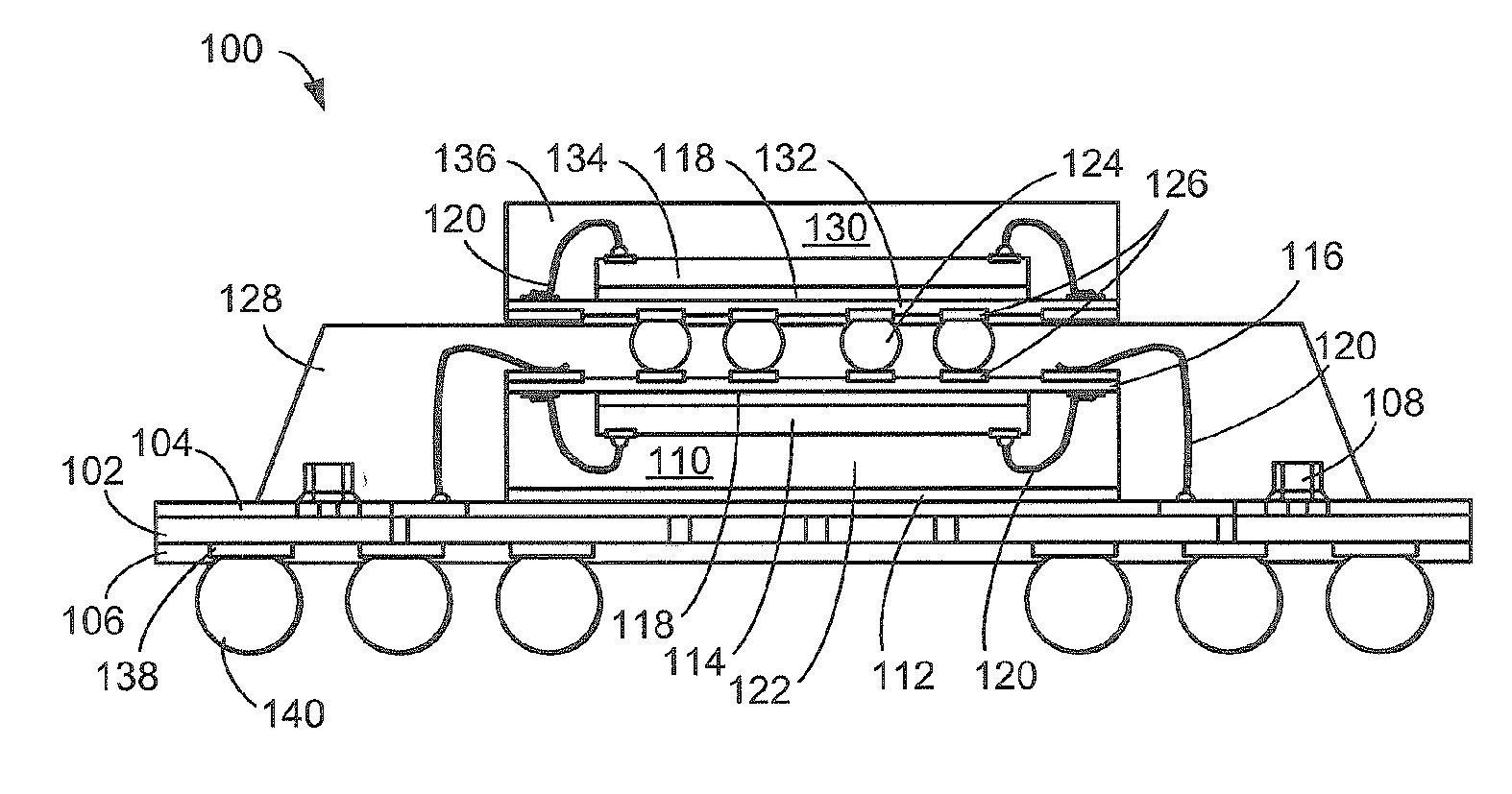
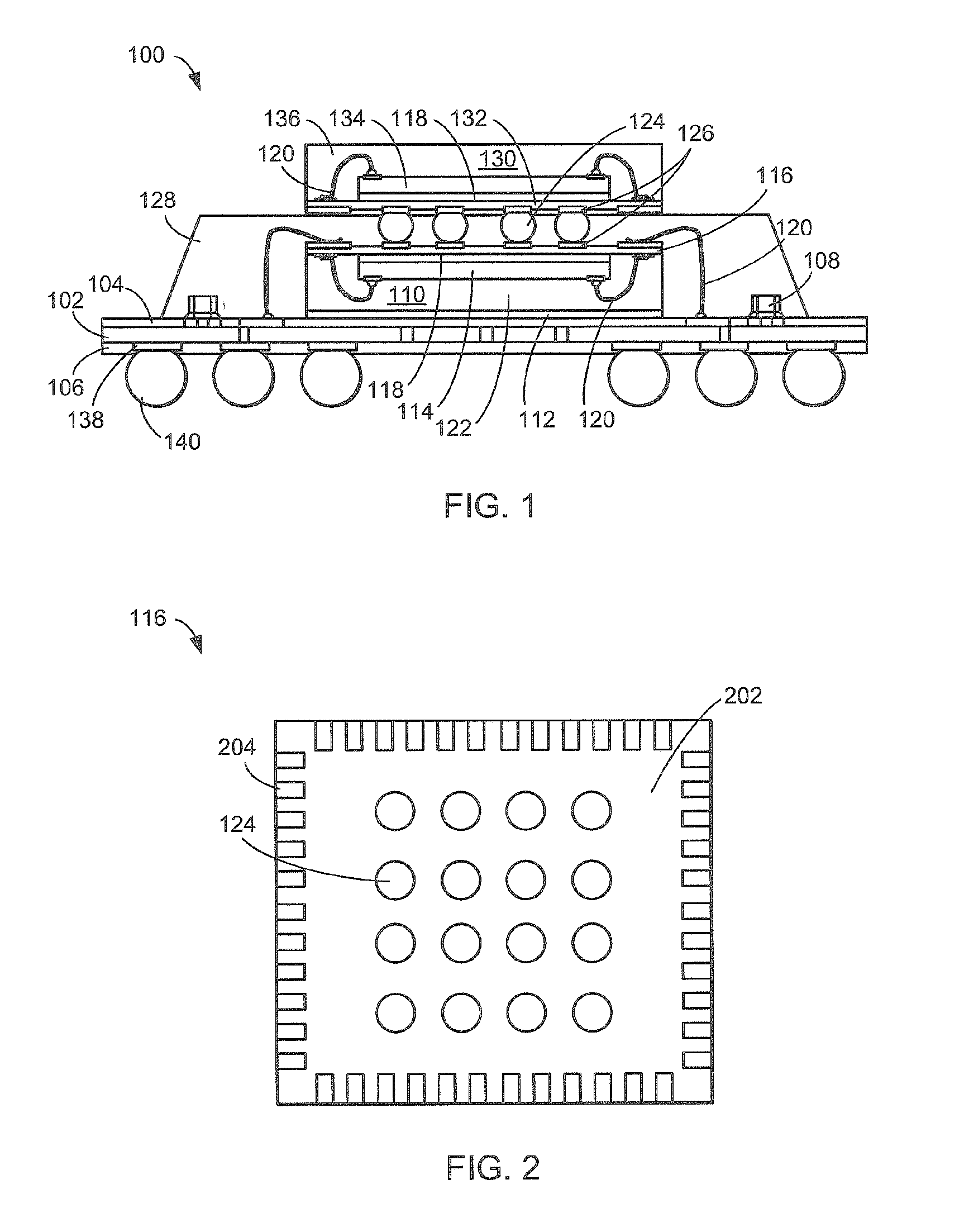
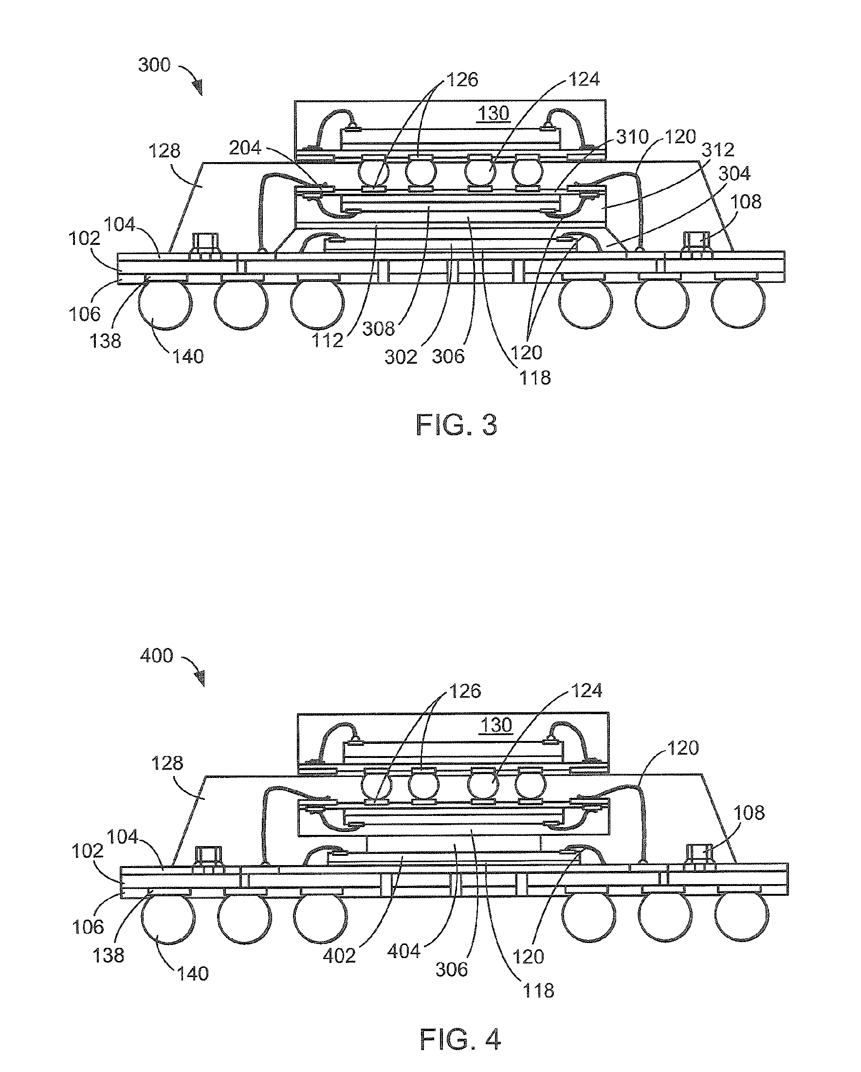
[0022] In the following description, numerous specific details are given to provide a thorough understanding of the invention. However, it will be apparent that the invention may be practiced without these specific details. In order to avoid obscuring the present invention, some well-known circuits, system configurations, and process steps are not disclosed in detail. Likewise, the drawings showing embodiments of the device are semi-diagrammatic and not to scale and, particularly, some of the dimensions are for the clarity of presentation and are shown greatly exaggerated in the drawing FIGs. In addition, where multiple embodiments are disclosed and described having some features in common, for clarity and ease of illustration, description, and comprehension thereof, the same numbers are used in all the drawing FIGs. to relate to the same elements.

[0023] The term “horizontal” as used herein is defined as a plane parallel to the conventional plane or surface of the attached die rega...


PUM


Abstract

The present invention provides a system for 3D package stacking system, comprising providing a substrate, attaching a ball grid array package, in an inverted position, to the substrate, forming a lower package, the lower package having the ball grid array package and the substrate encapsulated by a molding compound and attaching a second integrated circuit package over the lower package.

Description

CROSS-REFERENCE TO RELATED APPLICATIONS [0001] The present application contains subject matter related to a concurrently filed U.S. patent application Ser. No. 11 / 354,806, assigned to STATS ChipPAC Ltd. [0002] The present application contains subject matter related to co-pending U.S. patent application Ser. No. 11 / 306,627, assigned to STATS ChipPAC Ltd. [0003] The present application contains subject matter also related to co-pending U.S. patent application Ser. No. 11 / 306,628, assigned to STATS ChipPAC Ltd. [0004] The present application contains subject matter also related to co-pending U.S. patent application Ser. No. 11 / 326,211, assigned to STATS ChipPAC Ltd. [0005] The present application contains subject matter also related to co-pending U.S. patent application Ser. No. 11 / 326,206, assigned to STATS ChipPAC Ltd. TECHNICAL FIELD [0006] The present invention relates generally to integrated circuit package systems, and more particularly to a system for stacking 3D package structu...

Claims


Application Information

Patent Timeline
Patent Type & Authority Applications(United States)
IPC IPC(8): H01L23/48
CPCH01L23/3128H01L25/03H01L2924/19107H01L2224/73265H01L2224/73253H01L2224/73207H01L2224/48227H01L2224/32225H01L2224/16225H01L2225/1058H01L2225/1052H01L2225/1023H01L25/16H01L24/48H01L2924/19105H01L2924/19041H01L2924/15311H01L2924/14H01L25/105H01L2224/48091H01L2224/48465H01L2924/00014H01L2924/00H01L2924/00012H01L24/73H01L2924/181H01L2224/45099H01L2224/45015H01L2924/207
Inventor SHIM, IL KWONHAN, BYUNG JOONCHOW, SENG GUAN
Owner STATS CHIPPAC LTD
Why Eureka
Try Eureka