Optical deflecting device, optical deflecting device manufacturing method, and optical projecting device
- Summary
- Abstract
- Description
- Claims
- Application Information
AI Technical Summary
Benefits of technology
Problems solved by technology
Method used
Image

Examples
Embodiment Construction
[0052]Exemplary embodiments of the present invention are explained below. To avoid redundancy of explanation, in the drawings referred to in the following explanation, same portion or corresponding portions are provided with the same reference numerals.
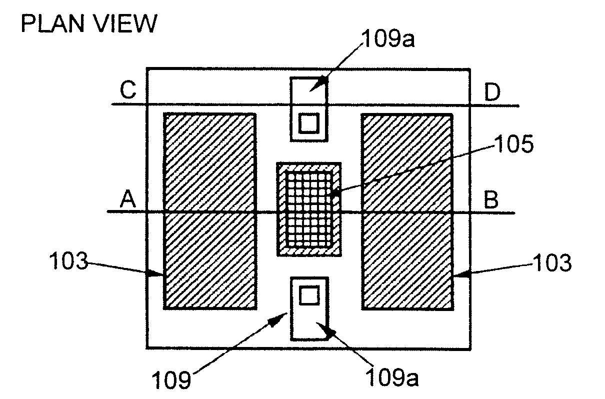
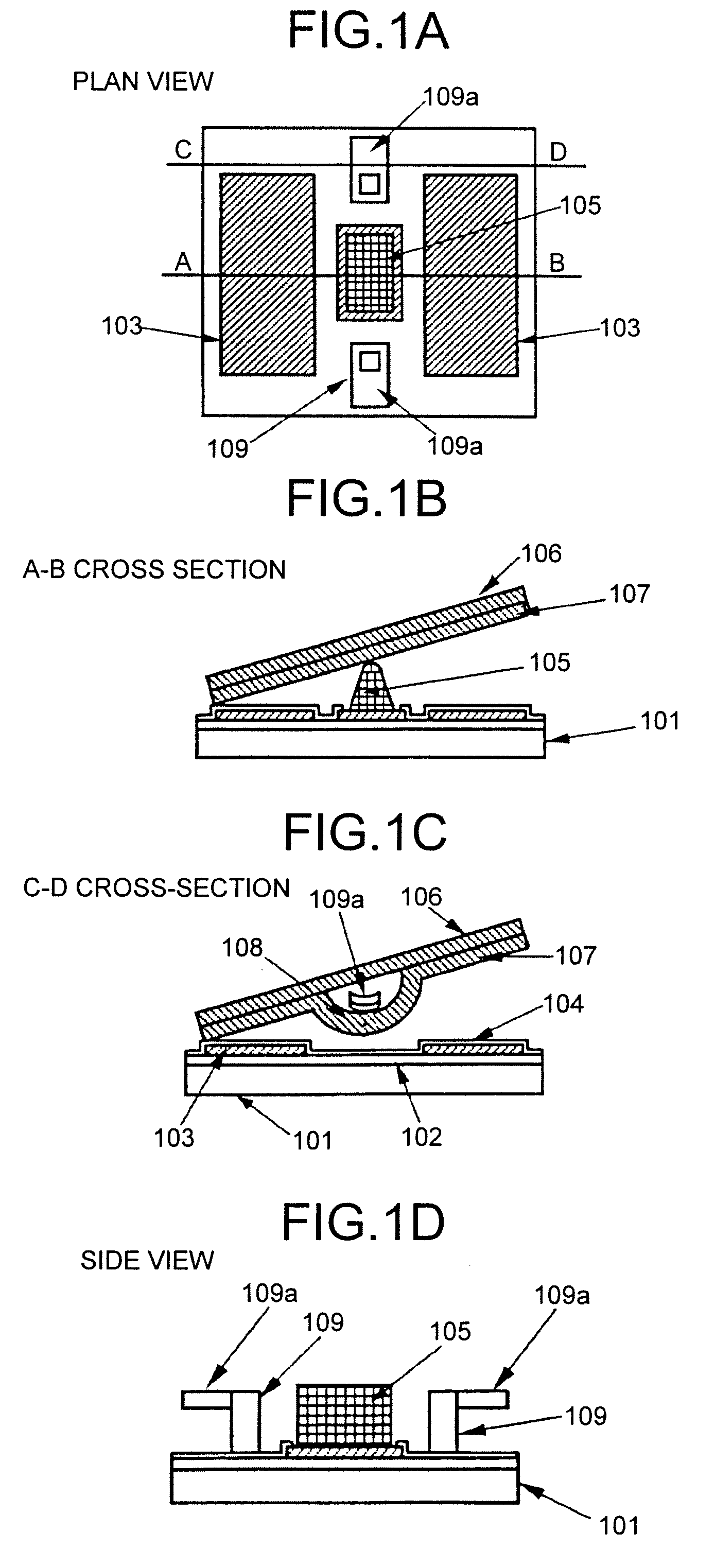
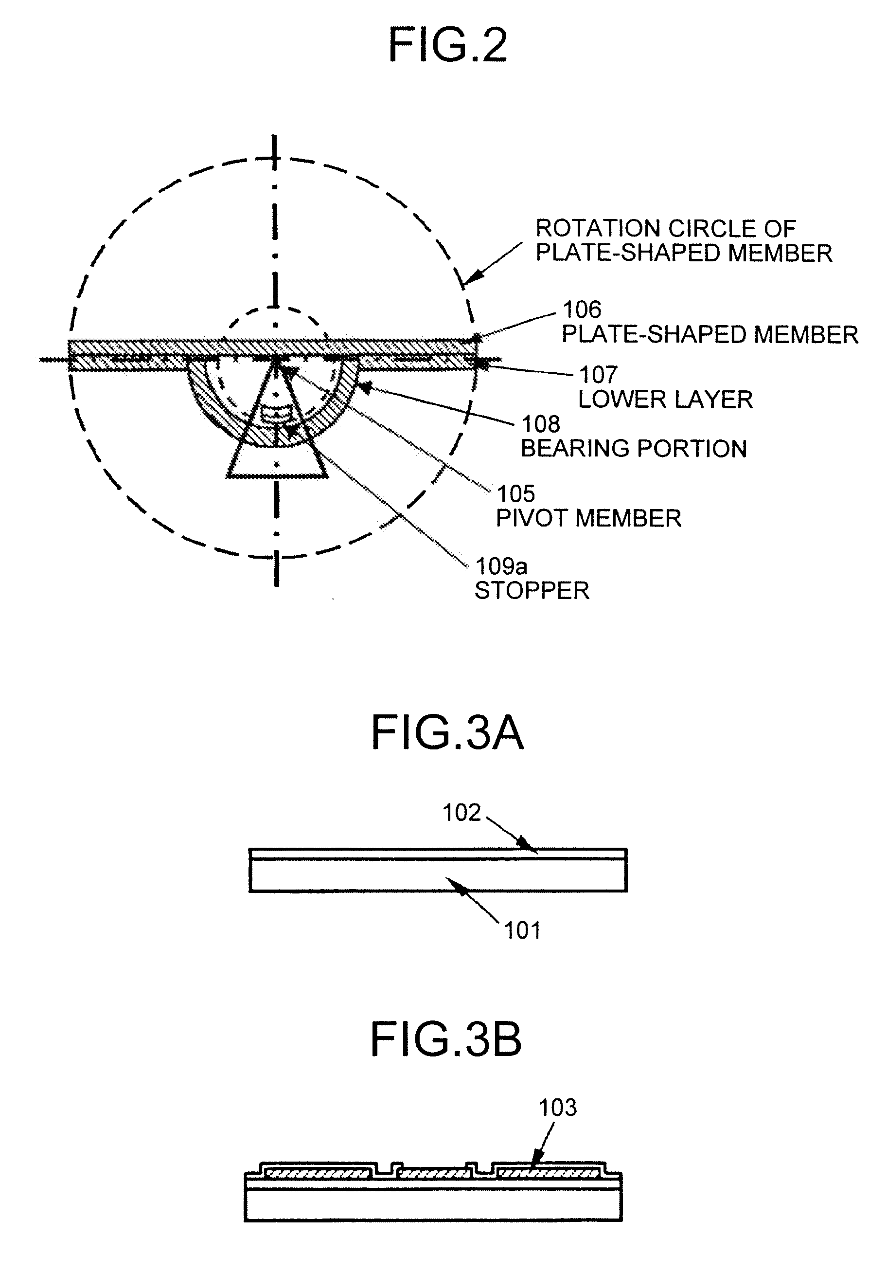
[0053]FIGS. 1A to 1D and 2 are drawings of the structure of an optical deflecting device according to the present embodiment. FIGS. 3A, 3B, and 4 to 12 are drawings for explaining an optical deflecting device manufacturing method according to the present embodiment.
[0054]FIG. 1A is a schematic plan view of the optical deflecting device (a plate-shaped member acting as a movable mirror is omitted). FIG. 1B is an A-B schematic cross-section view. FIG. 1C is a C-D schematic cross-section view. FIG. 1D is a schematic side view. Here, in FIG. 1A, the plate-shaped member acting as a movable mirror is omitted because it covers the entire surface. Also in FIG. 1D, the plate-shaped member is omitted.
[0055]The optical deflecting device accordin...
PUM
 Abstract
Description
Claims
Application Information
 - R&D Engineer
- R&D Manager
- IP Professional
- Industry Leading Data Capabilities
- Powerful AI technology
- Patent DNA Extraction
Browse by: Latest US Patents, China's latest patents, Technical Efficacy Thesaurus, Application Domain, Technology Topic.
© 2024 PatSnap. All rights reserved.Legal|Privacy policy|Modern Slavery Act Transparency Statement|Sitemap