Memory card having double contact pads and method for manufacturing the same
a memory card and contact pad technology, applied in the field of memory cards, can solve the problems of inconvenient memory card users and inability to operate properly
- Summary
- Abstract
- Description
- Claims
- Application Information
AI Technical Summary
Problems solved by technology
Method used
Image
Examples
Embodiment Construction
[0024]Embodiments of the present invention will be described below in more detail with reference to the accompanying drawings. The present invention may, however, be embodied in different forms and should not be construed as being limited to the embodiments set forth herein. Rather, these embodiments are provided so that this disclosure will be thorough and complete.
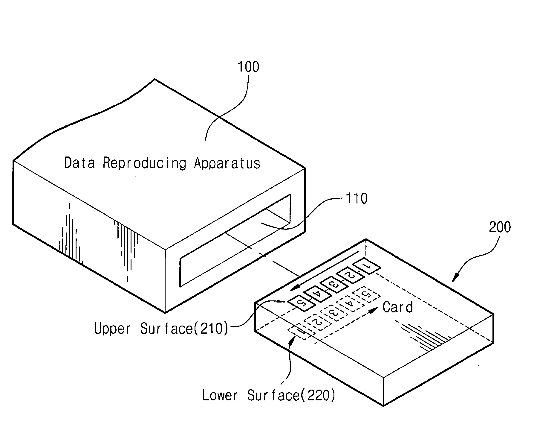
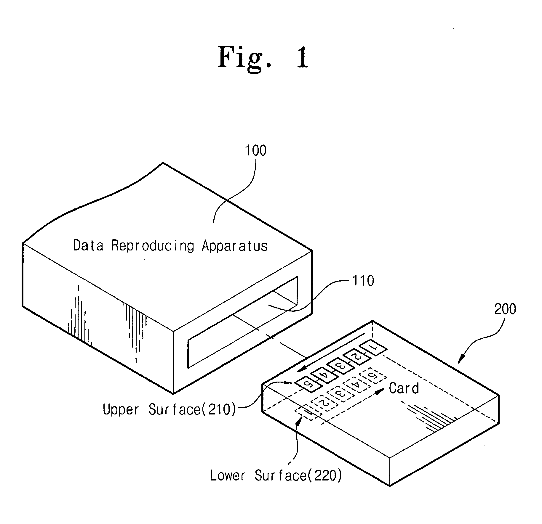
[0025]FIG. 1 is a schematic view illustrating a memory card according to an embodiment of the present invention. In the illustration of FIG. 1, the memory card 200 is being inserted into a data reproducing apparatus 100, host, or other device that is compatible with the memory card (collectively referred to hereinafter as a “data reproducing apparatus”).
[0026]The data reproducing apparatus 100 includes any apparatus capable of writing data to or reading data from the memory card 200. For example, the data reproducing apparatus 100 can include a computer, a digital camera, a mobile phone, a notebook, a personal digital as...
PUM
| Property | Measurement | Unit |
|---|---|---|
| electrical | aaaaa | aaaaa |
| structure | aaaaa | aaaaa |
| conductive | aaaaa | aaaaa |
Abstract
Description
Claims
Application Information


