Stackable circuit structures and methods of fabrication thereof

a technology of stackable circuits and circuit structures, applied in the direction of electrical equipment, semiconductor devices, semiconductor/solid-state device details, etc., can solve the problems of speed, and the conventional limit of process speed, and achieve the goal of providing electronic packaging and interconnects which provide maximum performance. , the problem of speed and size and interconnect density

Active Publication Date: 2011-06-23
EPIC TECH INC
View PDF56 Cites 198 Cited by
  • Summary
  • Abstract
  • Description
  • Claims
  • Application Information

AI Technical Summary

Benefits of technology

[0013]FIG. 1A is a plan view of one embodiment of a conventional integrated circuit chip with contact pads and redistribution pads (along the edge of the chip) shown interconnected by a redistribution metallization disposed over a dielectric layer;
[0014]FIG. 1B is a

Problems solved by technology

In recent years, this approach has met with problems of speed, size and interconnect density due to ever-constant demands for reduced size and increased performance from such integrated circuit packages.
Process speed is conventionally limited by the fact that individual packages have loading capacitance and inductance associated with their relatively long pins and by the large size of conductor runs in the packages relative to the size of the conductors of a bare IC chip.
As the speed of computers and other devices continues to increase, the problem of providing electronic packaging and interconnect which provides maximum performance has become a significant challenge.
One problem with

Method used


Image

  • Stackable circuit structures and methods of fabrication thereof
  • Stackable circuit structures and methods of fabrication thereof
  • Stackable circuit structures and methods of fabrication thereof

Examples


Embodiment Construction

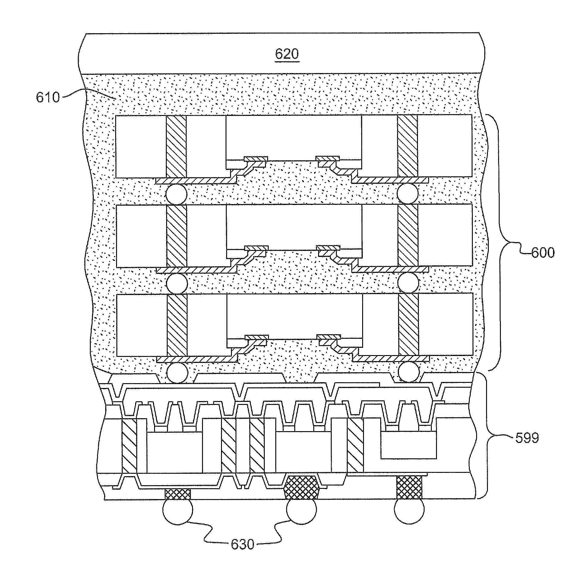
[0050]Generally stated, provided herein are numerous enhancements to multichip modules, and in particular, to chips-first circuit structures. Advantageously, described herein in one aspect are structures and fabrication methods for a chips-first circuit structure, or electronic module, wherein a first level metallization is applied directly to the front surface of the chips-first layer, without first applying a dielectric layer over the chips-first layer. Further, provided herein are structures and methods of fabrication which provide a chips-first circuit structure with a fan-out metallization from the chip pads, where lithography steps are minimized, and only one lithography step is used for the fan-out metallization. The structures and methods of fabrication described herein provide interconnect to a tight pad pitch, such as associated with today's integrated circuit chips, without the propensity for shorting to adjacent pads. This is accomplished by using (for example) the exist...


PUM


Abstract

Stackable circuit structures and methods of fabrication are provided employing first level metallization directly on a chips-first layer(s), which includes: a chip(s), each with a pad mask over its upper surface and openings exposing its contact pads; electrically conductive structures; and structural dielectric material surrounding the side surfaces of the chips and the conductive structures. Each chips-first layer further includes a metallization layer on the front surface of the layer, residing at least partially on the pad mask and extending over an edge of the chip. Together, the pad mask and the structural material electrically isolate the metallization layer from the chip. Input/output interconnect structures physically and electrically contact the metallization layer over the front surface and/or the lower surfaces of the electrically conductive structures at the back surface of the chips-first layer, to facilitate input/output connection to chips of the layers in a stack.

Description

TECHNICAL FIELD[0001]This invention relates in general to circuit structures and methods of fabrication thereof, and more particularly, to stackable (and stacked) chips-first circuit structures and methods of fabrication thereof.BACKGROUND OF THE INVENTION[0002]The conventional approach to electronic packaging and interconnect has been to package individual integrated circuit (IC) chips into a single package and to attach these packages to a printed circuit board to provide interconnect between the individual IC chips. In recent years, this approach has met with problems of speed, size and interconnect density due to ever-constant demands for reduced size and increased performance from such integrated circuit packages.[0003]Process speed is conventionally limited by the fact that individual packages have loading capacitance and inductance associated with their relatively long pins and by the large size of conductor runs in the packages relative to the size of the conductors of a bar...

Claims


Application Information

Patent Timeline
IPC IPC(8): H01L23/48H01L21/50
CPCH01L21/568H01L21/6835H01L23/49816H01L23/49827H01L23/5389H01L24/19H01L24/20H01L24/96H01L25/0655H01L25/0657H01L25/105H01L25/50H01L2221/68359H01L2224/04105H01L2224/12105H01L2224/131H01L2224/16146H01L2224/16237H01L2224/17181H01L2224/20H01L2224/2101H01L2224/2105H01L2224/211H01L2224/221H01L2224/48091H01L2224/48227H01L2224/73265H01L2224/97H01L2225/06513H01L2225/06517H01L2225/06582H01L2924/01011H01L2924/01013H01L2924/01018H01L2924/01027H01L2924/01029H01L2924/01042H01L2924/01074H01L2924/01078H01L2924/01079H01L2924/14H01L2924/15311H01L2924/18162H01L2924/19041H01L2924/30105H01L2924/30107H01L24/48H01L2924/01006H01L2924/01033H01L2924/014H01L2225/1035H01L2225/1058H01L2225/1082H01L2924/10253H01L2924/07811H01L2224/0401H01L2924/00014H01L2224/82H01L2924/00H01L2224/16225H01L2924/181H01L2224/45099H01L2224/45015H01L2924/207
Inventor KOHL, JAMES E.EICHELBERGER, CHARLES W.
Owner EPIC TECH INC
Why Eureka
Try Eureka