Thermal improvement for hotspots on dies in integrated circuit packages

a technology of integrated circuits and heat sinks, which is applied in the direction of semiconductor/solid-state device testing/measurement, semiconductor device details, semiconductor/solid-state device testing/measurement, etc., can solve the problems of power consumption, on-chip power dissipation will continue to rise, and the operating voltage cannot be reduced

Active Publication Date: 2007-12-20
AVAGO TECH INT SALES PTE LTD
View PDF91 Cites 193 Cited by
  • Summary
  • Abstract
  • Description
  • Claims
  • Application Information

AI Technical Summary

Benefits of technology

[0017]Methods and apparatuses for improved integrated circuit (IC) packages are described herein.

Problems solved by technology

Because of the increased difficulties in controlling noise margins as voltage decreases, operating voltages can no longer be reduced as quickly as in the past for 130 nm gate lengths and smaller.
Consequently, on-chip power dissipation will continue to rise.
With the increased use of 65 nm technology in foundry processes and the commercialization of 45 nm technology, power consumption is now a major technical problem facing the semiconductor industry.
Higher power density blocks create an uneven temperature distribution and lead to “hotspots,” also known as “hot blocks,” on the chip.
Also, if uniform carrier mobility is not achieved across the IC die due to on-chip temperature variations across the die, this may result in variations in signal speed and in complicating circuit timing control.
These methods are often ineffective and inadequate to reduce the temperature of the hotspots relative to the rest of the chip, such that operation of the chip is still limited by the hotspots.
Both the drop-in heat spreader and the external heat sink are ineffective to reduce the on-chip temperature differences caused by the hot spots.
These active cooling methods require exotic and expensive fluid circulation or micro-refrigeration systems and add to the total power consumption of the package that must be removed.
These can be costly and can decrease component reliability.
Because these solutions are typically expensive, their use is limited in cost sensitive applications such as consumer electronic devices.
These cooling methods as discussed above are inadequate and / or difficult and expensive to implement for commercial applications.

Method used


Image

  • Thermal improvement for hotspots on dies in integrated circuit packages
  • Thermal improvement for hotspots on dies in integrated circuit packages
  • Thermal improvement for hotspots on dies in integrated circuit packages

Examples


example bga embodiments

with Integrated Heat Spreader

[0071]FIGS. 3A-3E illustrate exemplary embodiments of molded plastic fine pitch ball grid array (BGA) packages having a heat spreader 302 which is at least partially covered by mold compound 112. In the embodiments of FIGS. 3A-3E, the configuration of heat spreader 302 is varied from package to package.

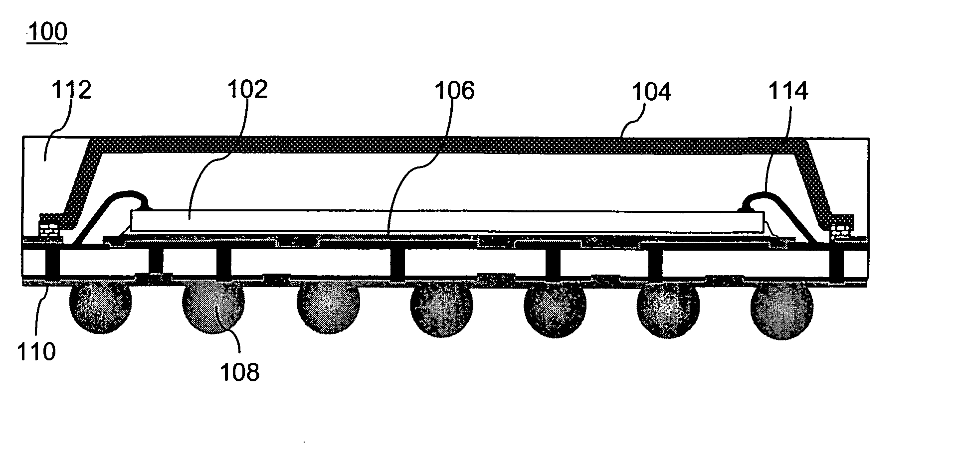
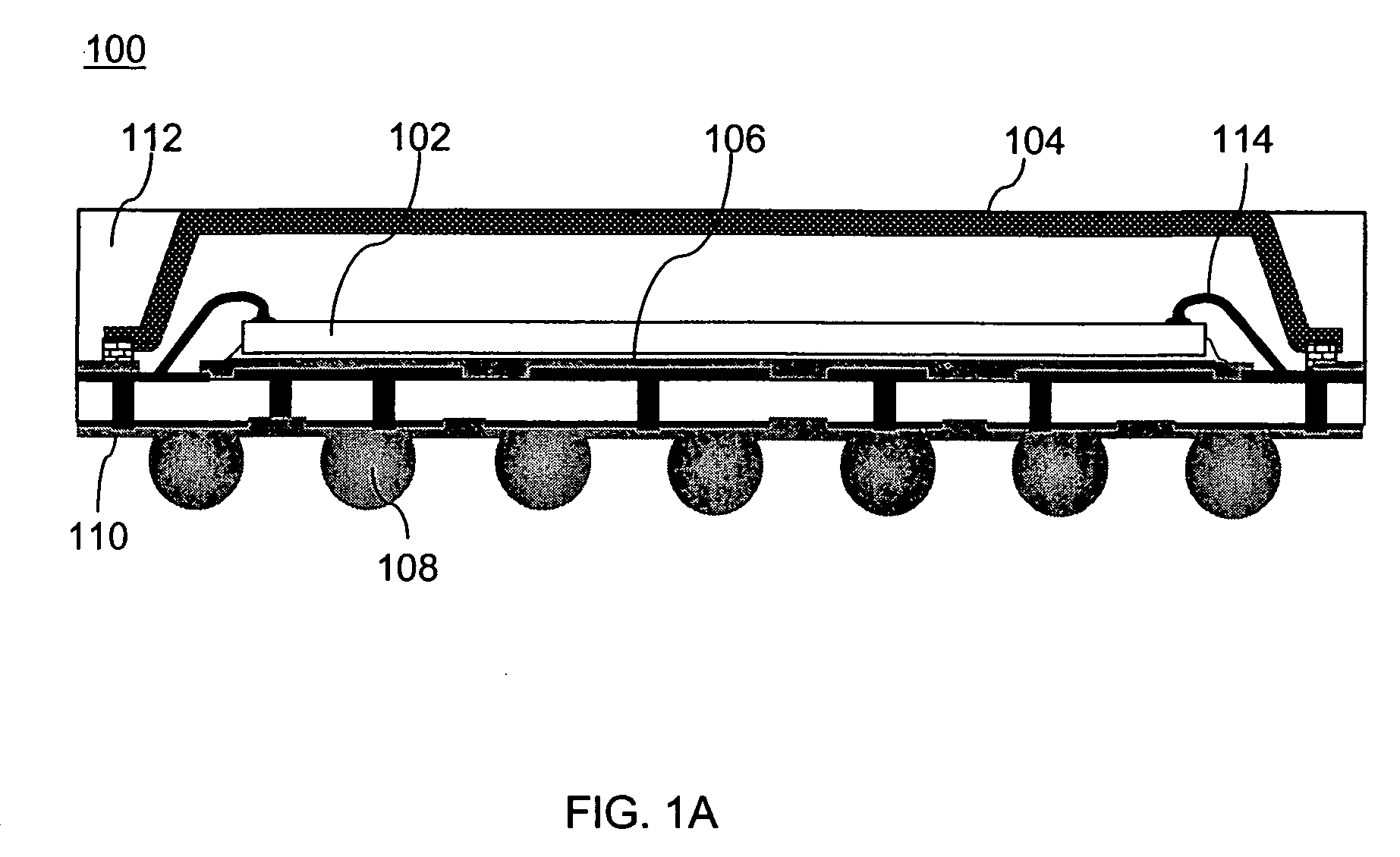
[0072]For example, FIG. 3A illustrates a package 300 having a planar heat spreader 302 integrated with package 300 in a partially embedded manner, having a planar top surface 304 of heat spreader 302 exposed (not covered by mold compound 112). In package 300, IC die 102 is electrically interconnected to substrate 110 by one or more wire bonds 114. One or more thermal interconnect members 208 are attached to the top surface of die 102. Mold compound 112 encapsulates die 102, wire bonds 114, a top surface of substrate 110, and thermal interconnect members 208. In an embodiment, mold compound 112 can be formed on substrate 110 using a mold process, a saw sing...


PUM


Abstract

Methods and apparatuses for improved integrated circuit (IC) packages are described herein. In an aspect, an IC device package includes an IC die having a contact pad, where the contact pad is located on a hotspot of the IC die. The hotspot is thermally coupled to a thermal interconnect member. In an aspect, the package is encapsulated in a mold compound. In a further aspect, a heat spreader is attached to the mold compound, and is thermally coupled to the thermal interconnect member. In another aspect, a thermal interconnect member thermally is coupled between the heat spreader and the substrate.

Description

[0001]This application claims the benefit of U.S. Provisional Appl. No. 60 / 814,876, filed Jun. 20, 2006, which is herein incorporated by reference in its entirety.BACKGROUND OF THE INVENTION[0002]1. Field of the Invention[0003]The invention relates generally to the field of integrated circuit (IC) device packaging technology, and more particularly to the cooling of hotspots on IC semiconductor die, heat spreading for IC packages, and thermal interconnection technology in IC packaging.[0004]2. Background Art[0005]Electronic signals are carried by electrical current through conductors and transistors in a large scale integrated circuit (IC) fabricated on semiconductor substrate. The energy carried by the electrical current is partially dissipated along the paths of current flow through the IC in the form of heat. Heat generation in electronic semiconductor ICs is also known as power consumption, power dissipation, or heat dissipation. The heat generated, P, in an IC is the sum of dyna...

Claims


Application Information

Patent Timeline
Patent Type & Authority Applications(United States)
IPC IPC(8): H01L23/48
CPCH01L23/367H01L2924/12041H01L23/49816H01L24/73H01L2224/2919H01L2224/48091H01L2224/48227H01L2224/48247H01L2224/48257H01L2224/48465H01L2224/73265H01L2224/83101H01L2924/01013H01L2924/01029H01L2924/01033H01L2924/01046H01L2924/01077H01L2924/01078H01L2924/01079H01L2924/01082H01L2924/10253H01L2924/16152H01L2924/3025H01L23/4334H01L2924/1815H01L2924/15311H01L2924/01322H01L2924/01074H01L2924/01047H01L2924/01023H01L2924/01006H01L2924/01005H01L2224/32245H01L24/48H01L2224/32225H01L2924/0665H01L2924/00014H01L2924/00012H01L2924/00H01L2924/181H01L2224/85H01L2924/12042H01L2224/45099H01L2224/85399H01L2224/05599H01L23/40H01L21/565H01L22/10H01L23/315H01L23/3675H01L24/17H01L24/81H01L24/85H01L2224/16113H01L2224/16245H01L2224/17519H01L2224/48106H01L2224/48157H01L2224/81897H01L2924/14
Inventor ZHAO, SAM ZIQUNKHAN, REZAUR RAHMAN
Owner AVAGO TECH INT SALES PTE LTD
Why Eureka
Try Eureka