Semiconductor module with a semiconductor stack, and methods for its production

a technology of semiconductor stack and semiconductor module, which is applied in the direction of semiconductor devices, semiconductor/solid-state device details, electrical apparatus, etc., can solve the problems of occupying a large amount of space, reducing the reliability of known semiconductor modules, and the height of the module cannot be reduced indefinitely

Inactive Publication Date: 2005-06-23
INFINEON TECH AG
View PDF14 Cites 203 Cited by
  • Summary
  • Abstract
  • Description
  • Claims
  • Application Information

AI Technical Summary

Benefits of technology

[0005] One object of the invention is to overcome the previously noted disadvantages and to provide a reliable semiconductor module with...

Problems solved by technology

One disadvantage of this known semiconductor module is the large number of at least three connecting interfaces between the three substrates and the connecting frame, which on the one hand must be adjusted with respect to one another and on the other hand must be electrically connected to one another, thus ...

Method used


Image

  • Semiconductor module with a semiconductor stack, and methods for its production
  • Semiconductor module with a semiconductor stack, and methods for its production
  • Semiconductor module with a semiconductor stack, and methods for its production

Examples


first embodiment

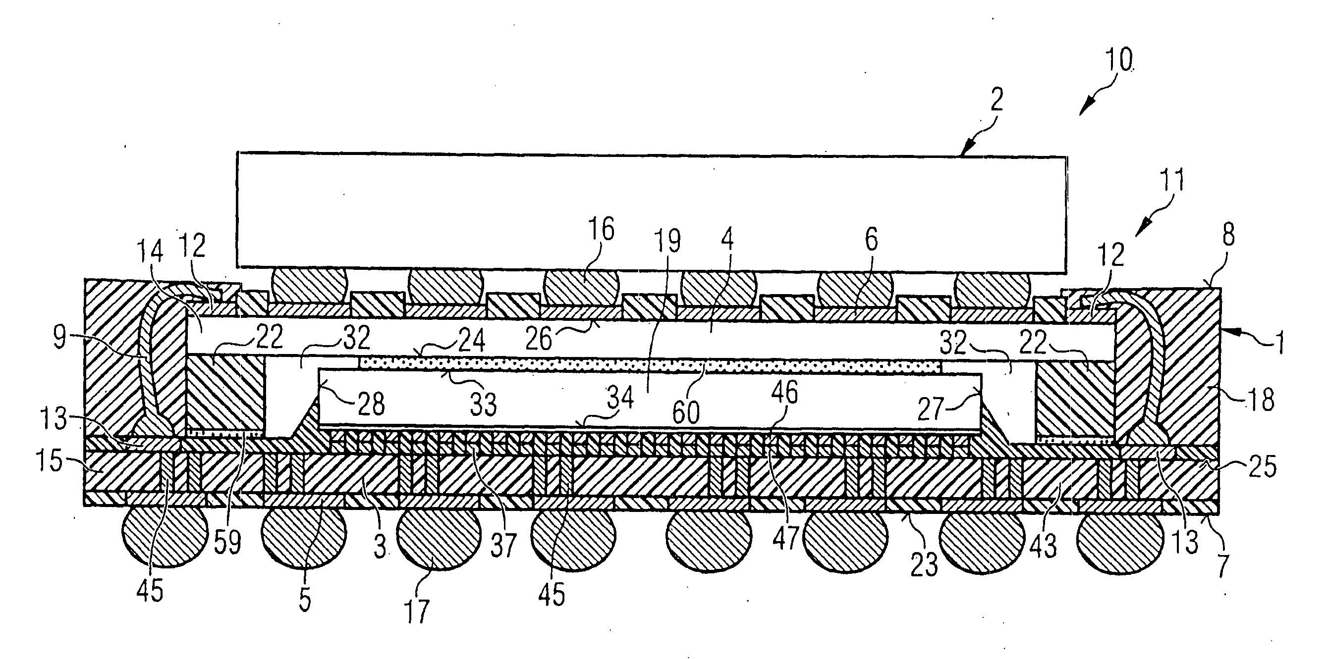
[0046]FIG. 1 shows a schematic cross-sectional view of a semiconductor module 10 with a semiconductor stack 11, according to the invention. This first variant of the invention uses a so-called interposer as the upper interposing unit 4 with moulded spacers 22. This variant is preferably used for a basic component 1 with a semiconductor chip 19 which has flipchip contacts 46. The flipchip contacts 46 are fit to contact connecting pads 47 on a lower interposing unit 3. Semiconductor chips 19 such as these with flipchip contacts 46 have a smaller area than the area which is required for the upper interposing unit 4, or for an interposer. The spacers 22 are used to support the areas in which a wire bond must be passed through, thus allowing a reliable bonding process. After wire bonding, the bonding channels are closed by means of an encapsulating process by means of moulding or dispensing, with the bonding connections 9 being embedded. This configuration, as is shown in FIG. 1, may als...

second embodiment

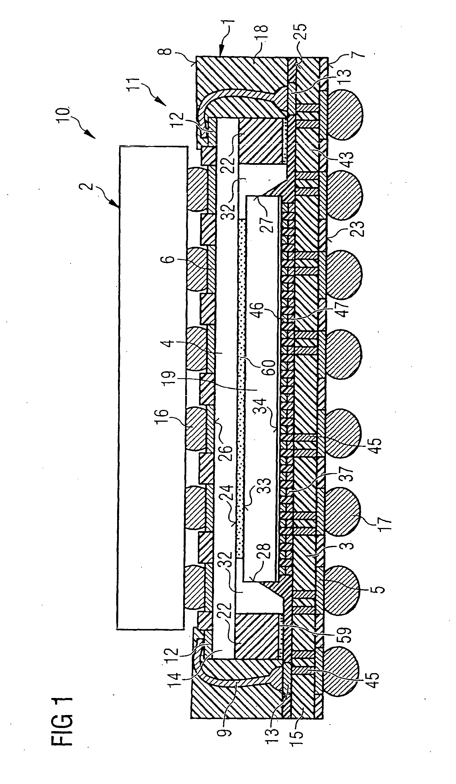
[0053]FIG. 2 shows a schematic cross-sectional view of a semiconductor module 20 with a semiconductor stack 21 according to the invention.

[0054] Components with the same functions are identified by the same reference symbols as in FIG. 1, and will not be explained again.

[0055] This second embodiment or second variant is similar to the first embodiment. However, in the second embodiment, not only are the channels with the bonding wires located in them encapsulated, with the bonding connections 9 thus being embedded in a plastic housing compound 18, but the cavities 32, as can also be seen in FIG. 1, underneath the upper interposing board are also filled with the encapsulation compound, such as a plastic housing compound 18. This is achieved by the spacer 22 not completely surrounding the semiconductor chip 29 of the basic semiconductor component 1 but, in fact, being arranged only on the two opposite edge faces of the semiconductor chips 27 and 28, so that the plastic housing compou...

third embodiment

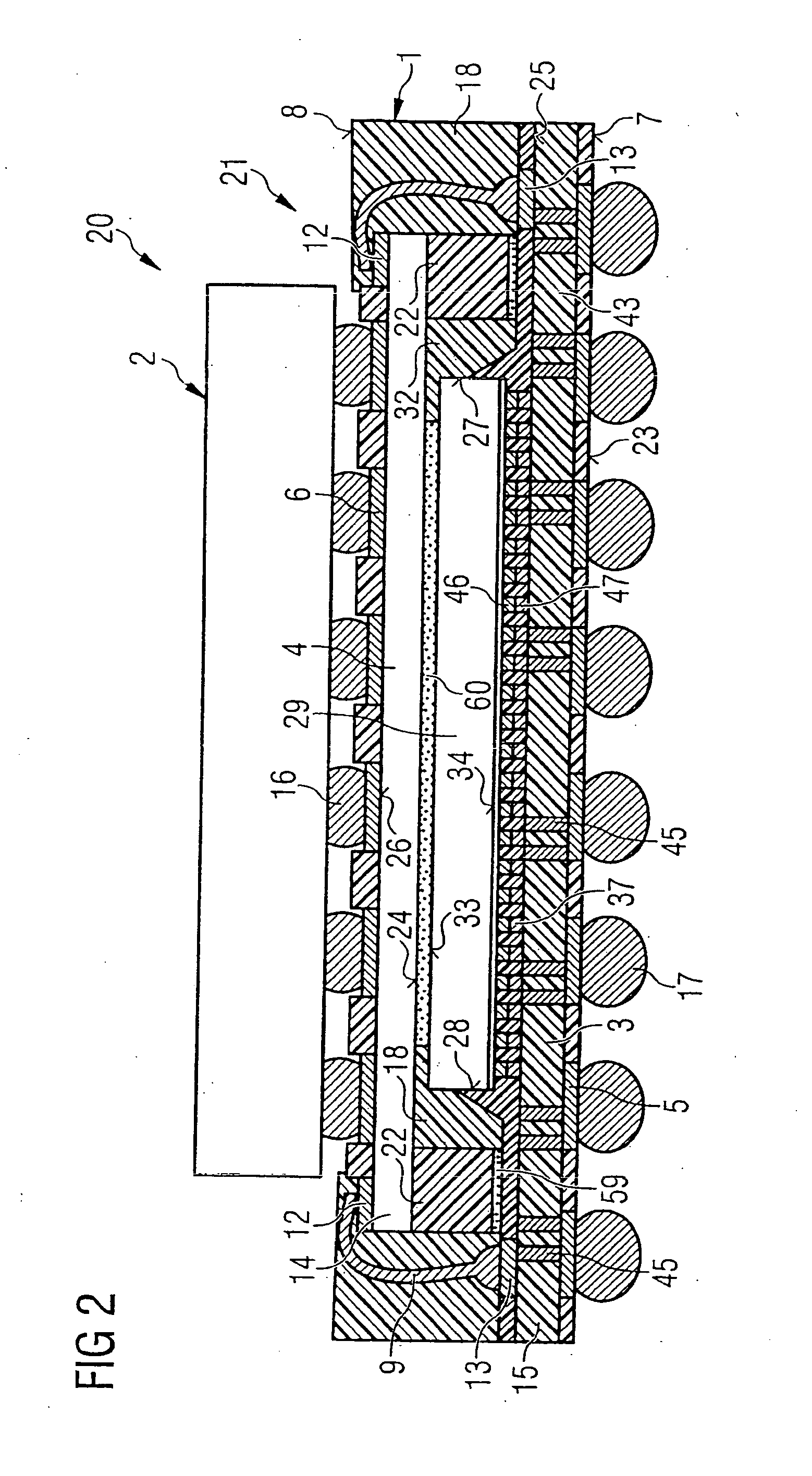
[0057]FIG. 3 shows a schematic cross-sectional view of a semiconductor module 30 with a semiconductor stack 31, according to the invention. Components with the same functions as in FIG. 1 are identified by the same reference symbols, and will not be explained again.

[0058] In this third variant or third embodiment of the invention as depicted in FIG. 3, an upper interposing unit 4 or else an interposer is used without any further spacers (e.g., without spacers 22 as depicted in the embodiments of FIGS. 1 and 2). This variant may be used when the upper interposing unit 4 has a surface which corresponds approximately to the semiconductor chip 39 between the upper interposing unit 4 and the lower interposing unit 3.

[0059] In this case, the forces which occur during production of the bonding connections 9 are absorbed in a supporting manner by the semiconductor chip 39 itself, so that the semiconductor chip 39 contributes to making the edge areas 14 of the upper interposing unit 4 (whic...


PUM


Abstract

An electronic semiconductor module component with a semiconductor stack includes semiconductor components arranged in a vertically stacked relationship. A basic semiconductor component includes a lower interposing unit, on which lower external contact pads are arranged. The basic semiconductor component further includes an upper interposing unit, on which upper external contact pads are arranged. The two interposing units are electrically connected to one another via bonding connections disposed at their edge areas. The basic semiconductor component is a compact component on which different, customer-specific semiconductor components can be stacked.

Description

CROSS REFERENCE TO RELATED APPLICATIONS [0001] This application claims priority under 35 USC §119 to German Application No. DE 103 60 708.0, filed on Dec. 19, 2003, and titled “Semiconductor Module with a Semiconductor Stack, and Methods for its Production,” the entire contents of which are hereby incorporated by reference.FIELD OF THE INVENTION [0002] The invention relates to a semiconductor module with a semiconductor stack, and to methods for its production. BACKGROUND [0003] A semiconductor module such as the type described in U.S. patent application Publication No. 2001 / 0054770 A1 and, for stacking purposes, uses a complex connecting frame and two additional basic layers, which each have a basic substrate and a wiring pattern. The connecting frame has vias from one of the basic substrates to the other basic substrate. Integrated semiconductor chips are electrically connected to the basic substrates and to their interposing patterns in such a way that a first semiconductor chip ...

Claims


Application Information

Patent Timeline
IPC IPC(8): H01L23/12H01L21/56H01L23/00H01L23/04H01L23/31H01L23/498H01L25/10
CPCH01L21/563H01L23/04H01L23/3128H01L23/49833H01L24/97H01L25/105H01L2224/48471H01L2224/73204H01L2224/73253H01L2224/73265H01L2224/83051H01L2224/97H01L2924/01082H01L2924/15311H01L2924/16195H01L2924/19107H01L2224/16225H01L2224/32225H01L2224/48227H01L24/48H01L2924/01005H01L2924/01006H01L2924/01033H01L2924/01068H01L2225/1023H01L2225/1041H01L2225/1058H01L2224/32145H01L2224/16235H01L2224/85H01L2224/81H01L2924/00H01L2924/00012H01L24/73H01L2924/00014H01L2924/181H01L2224/45099H01L2224/45015H01L2924/207H01L23/00H01L23/12
Inventor POHL, JENSROEMER, BERNDSCHAETZLER, BERNHARDSTUEMPFL, CHRISTIANVILSMEIER, HERMANWOERNER, HOLGERZUHR, BERNHARD
Owner INFINEON TECH AG
Why Eureka
Try Eureka