
Thermoelectric converter and method of manufacturing thermoelectric converter

Inactive Publication Date: 2008-09-18
IBIDEN CO LTD
View PDF15 Cites 16 Cited by
  • Summary
  • Abstract
  • Description
  • Claims
  • Application Information

AI Technical Summary

Problems solved by technology

However, a thermoelectric conversion module into which a large number of such thermoelectric conversion elements are combined is a static thermoelectric converter characterized by no movable parts to cause vibration, noise, wear, etc., simple structure and high reliability, and a long service life and easy maintenance.
However, many of these semiconductors contain harmful metal, so that attention is required in both their manufacture and use.
However, it is accompanied by manufacturing complexity to accurately arrange minute semiconductor elements in accordance with a desired arrangement pattern and form electrodes at both ends.
Further, there is also a problem in that a completed module is mechanically weak.

Method used


Image

  • Thermoelectric converter and method of manufacturing thermoelectric converter
  • Thermoelectric converter and method of manufacturing thermoelectric converter
  • Thermoelectric converter and method of manufacturing thermoelectric converter

Examples


Embodiment Construction

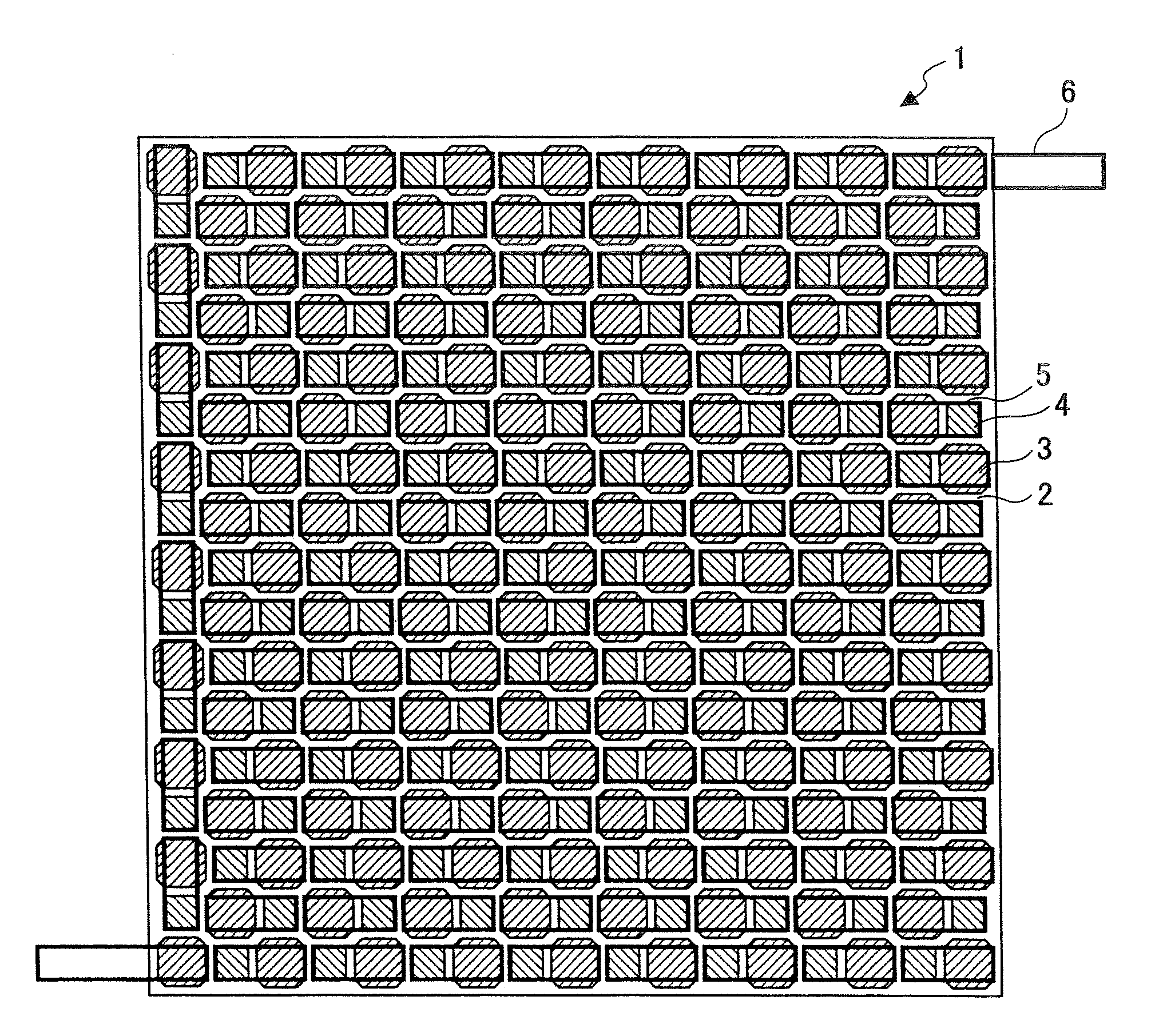
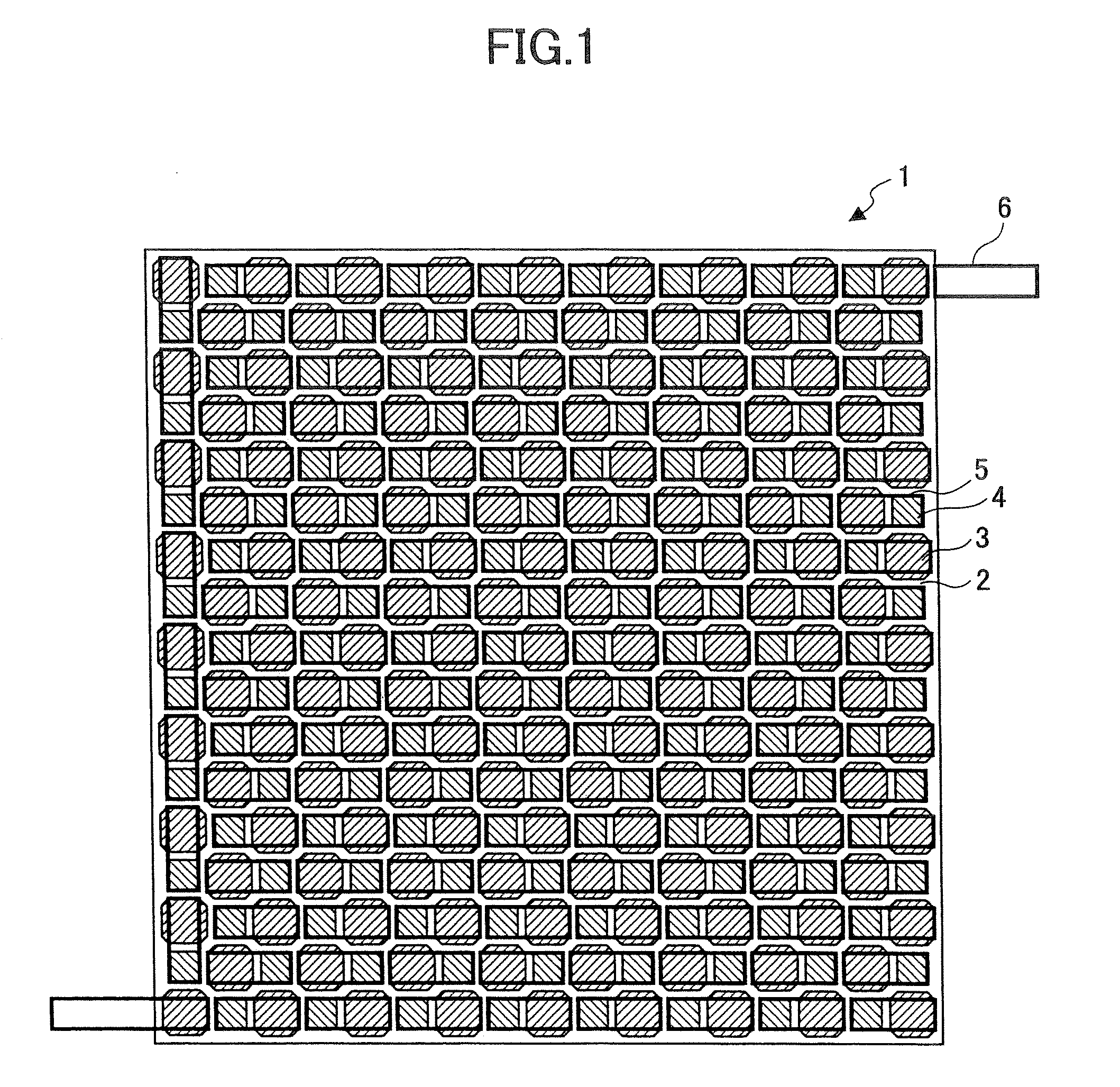
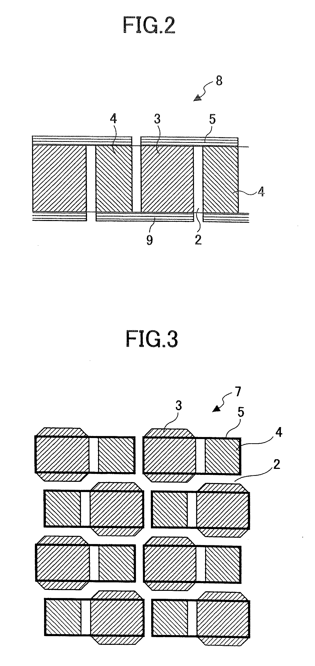
[0028]In a thermoelectric converter according to one embodiment of the present invention, p-type semiconductors and n-type semiconductors are alternately provided in corresponding first and second through holes, respectively, in a ceramic honeycomb, the first and second through holes having different cross-sectional shapes and being alternately arranged, and the semiconductors have respective first and second ends thereof successively connected to different ones of the semiconductors on first and second sides, respectively, of the corresponding through holes.

[0029]According to one embodiment of the present invention, there is provided a method of manufacturing a thermoelectric converter including the steps of (a) arranging first and second through holes having different cross-sectional shapes alternately in a ceramic honeycomb, (b) providing p-type semiconductors and n-type semiconductors alternately in the corresponding first and second through holes, respectively, of the ceramic h...


PUM


Abstract

A thermoelectric converter including p-type semiconductors and n-type semiconductors alternately provided in corresponding first and second through holes, respectively, in a ceramic honeycomb. The first and second through holes have different cross-sectional shapes and are alternately arranged. The semiconductors have respective first and second ends thereof successively connected to different ones of the semiconductors on first and second sides, respectively, of the corresponding through holes.

Description

CROSS-REFERENCE TO RELATED APPLICATION[0001]The present application is based on PCT International Application No. PCT / JP2007 / 055259, filed on Mar. 15, 2007, the entire contents of which are hereby incorporated by reference.BACKGROUND OF THE INVENTION[0002]1. Field of the Invention[0003]The present invention relates to a thermoelectric converter and a method of manufacturing the thermoelectric converter.[0004]2. Description of the Related Art[0005]When one end of a p-type semiconductor and one end of an n-type semiconductor are joined through an electrode, and this junction is set at high temperature while the other end of each of the p-type semiconductor and the n-type semiconductor is set at low temperature, an electromotive force is generated between the ends of each of the p-type semiconductor and the n-type semiconductor in accordance with the difference in temperature between the high temperature part and the low temperature part. The electromotive force generated between the e...

Claims


Application Information

Patent Timeline
IPC IPC(8): H01L35/16H01L35/22H01L21/00
CPCH01L35/32H10N10/17
Inventor OHNO, KAZUSHIGE
Owner IBIDEN CO LTD
Learn More