Field barrier structures within a conformal shield

a field barrier and conformal shield technology, applied in the direction of semiconductor/solid-state device details, cross-talk/noise/interference reduction, printed circuit manufacturing, etc., can solve the problem that emissions may interfere with the operation of an electronic component subject to emissions, and similar electrical shorts occur

Inactive Publication Date: 2009-01-01
RF MICRO DEVICES
View PDF97 Cites 71 Cited by
  • Summary
  • Abstract
  • Description
  • Claims
  • Application Information

AI Technical Summary

Benefits of technology

[0007]The present invention may be used to form one or more shields for corresponding component areas of a given module. In one embodiment, a meta-module having circuitry for two or more modules is formed on a substrate, which is preferably a laminated substrate. As such, the circuitry for the different modules is initially formed on the single meta-module. Each module will have one or more component areas in which the circuitry is formed. A metallic structure is formed on or in the substrate for each component area to be shielded on the substrate. In one embodiment, each metallic structure extends about all or a portion of the periphery of each of the component areas to be shielded. A single body, such as an overmold body, is then formed over all of the modules on the meta-module. After the body is formed, at least a portion of the metallic structure for each component area to be shielded is exposed through the body by a cutting, drilling, or like operation. Next, an electromagnetic shield material is applied to the exterior surface of the body of each of the component areas to be shielded and in contact with the exposed portion of the metallic structures. The modules are then singulated from each other to form separate modules, each of which having one or more integrally shielded component areas.

Problems solved by technology

While the benefits of these devices are myriad, smaller electronic components that operate at higher frequencies also create problems.
If the signal strengths of the emissions are high enough, the emissions may interfere with the operation of an electronic component subjected to the emissions.
Likewise, when external emissions from outside the shield strike the exterior surface of the shield, a similar electrical short occurs, and the electronic components on the module do not experience the emissions.
However, as modules continue to become smaller from miniaturization, creating effective shields that do not materially add to the size of the module becomes more difficult.

Method used


Image

  • Field barrier structures within a conformal shield
  • Field barrier structures within a conformal shield
  • Field barrier structures within a conformal shield

Examples


Embodiment Construction

[0047]The embodiments set forth below represent the necessary information to enable those skilled in the art to practice the invention and illustrate the best mode of practicing the invention. Upon reading the following description in light of the accompanying drawing figures, those skilled in the art will understand the concepts of the invention and will recognize applications of these concepts not particularly addressed herein. It should be understood that these concepts and applications fall within the scope of the disclosure and the accompanying claims.

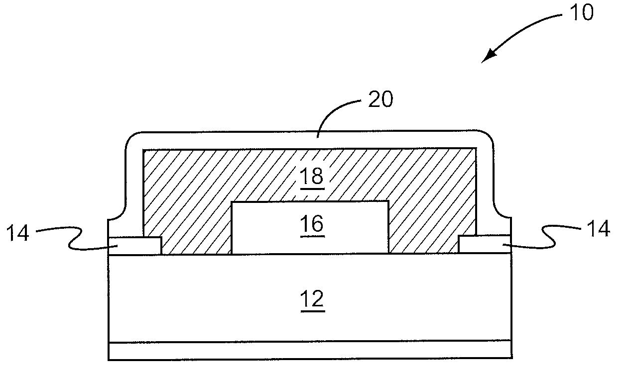
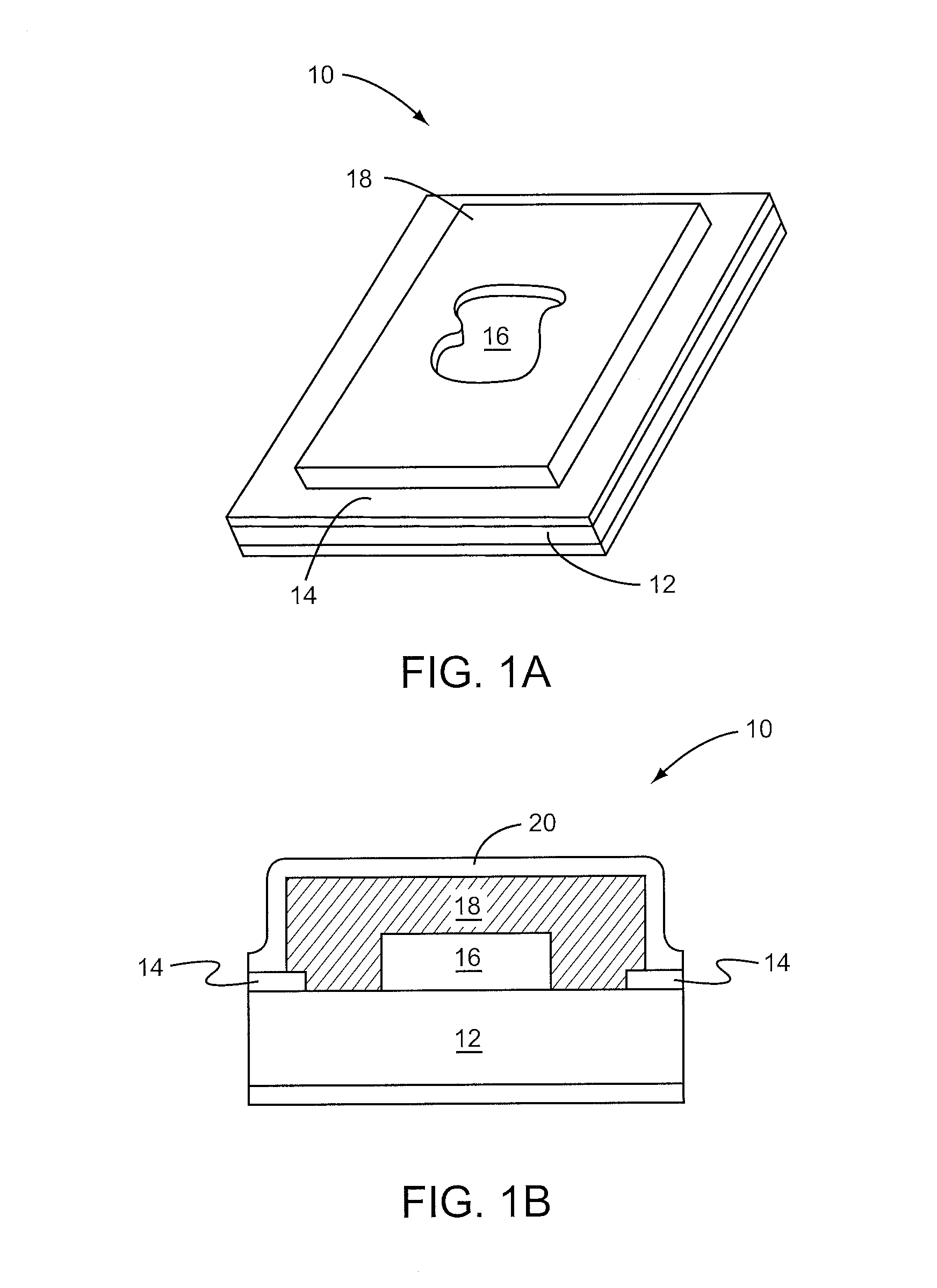
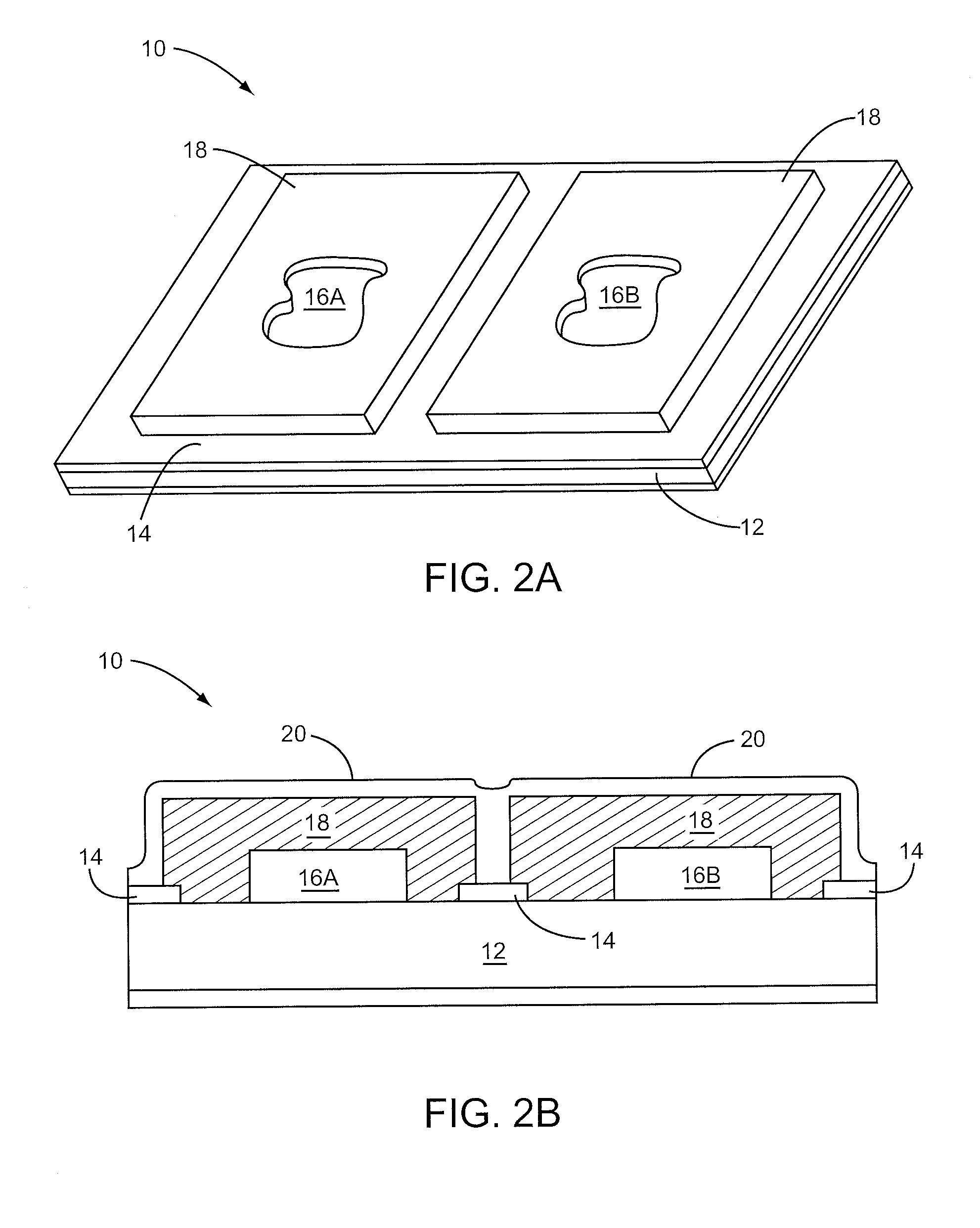
[0048]The present invention may be used to form one or more shields for corresponding component areas of a given module. In one embodiment, a meta-module having circuitry for two or more modules is formed on a substrate, which is preferably a laminated substrate. As such, the circuitry for the different modules is initially formed on the single meta-module. Each module will have one or more component areas in which the circuitry i...


PUM

PropertyMeasurementUnit
thickaaaaaaaaaa
metallic structuresaaaaaaaaaa
conductiveaaaaaaaaaa

Abstract

In one embodiment, a meta-module having circuitry for two or more modules is formed on a substrate, which is preferably a laminated substrate. The circuitry for the different modules is initially formed on the single meta-module. Each module will have one or more component areas in which the circuitry is formed. A metallic structure is formed on or in the substrate for each component area to be shielded. A single body, such as an overmold body, is then formed over all of the modules on the meta-module. At least a portion of the metallic structure for each component area to be shielded is then exposed through the body by a cutting, drilling, or like operation. Next, an electromagnetic shield material is applied to the exterior surface of the body of each of the component areas to be shielded and in contact with the exposed portion of the metallic structures.

Description

[0001]This application claims the benefit of U.S. provisional patent applications 60 / 946,453 filed Jun. 27, 2007 and 60 / 978,006 filed Oct. 5, 2007, the disclosures of which are incorporated herein by reference in their entireties.CROSS-REFERENCE TO RELATED APPLICATIONS[0002]This application is related to U.S. utility patent application Ser. No. 11 / 199,319 filed Aug. 8, 2005 and U.S. utility patent application Ser. No. 11 / 435,913 filed May 17, 2006, the disclosures of which are incorporated herein by reference in their entireties. This application is also related to the following concurrently filed U.S. patent applications: application Ser. No. ______ entitled ISOLATED CONFORMAL SHIELDING; application Ser. No. ______ entitled CONFORMAL SHIELDING EMPLOYING SEGMENT BUILDUP; application Ser. No. ______ entitled CONFORMAL SHIELDING PROCESS USING FLUSH STRUCTURES; application Ser. No. ______ entitled HEAT SINK FORMED WITH CONFORMAL SHIELD; application Ser. No. ______ entitled CONFORMAL SH...

Claims


Application Information

Patent Timeline
Patent Type & Authority Applications(United States)
IPC IPC(8): H05K9/00
CPCH01L23/552Y10T29/49128H01L2924/01013H01L2924/01016H01L2924/01018H01L2924/01029H01L2924/0103H01L2924/01033H01L2924/01046H01L2924/01047H01L2924/01078H01L2924/01079H01L2924/01082H01L2924/14H01L2924/1815H01L2924/3025H05K1/0218H05K3/0052H05K3/181H05K3/284H05K2203/0723H01L2924/01005H01L2924/01006H01L2924/014H01L2924/12041H01L25/0655Y10T29/4913Y10T29/49789Y10T29/49124Y10T29/49002Y10T29/49204Y10T29/49131Y10T29/49126Y10T29/49155Y10T29/49Y10T29/49144Y10T29/49117Y10T29/49153Y10T29/49146H01L24/97
Inventor MADSEN, ULRIK RIISUBBESEN, LARS SANDAHL
Owner RF MICRO DEVICES
Why Eureka
Try Eureka