Methods and Apparatuses for Flushing Write-Combined Data From A Buffer

a write-combined data and buffer technology, applied in the field of integrated circuit and computer system design, can solve the problems of premature flushing of write-combined buffers, processor write-combining making no guarantees with respect to the order in which bits are written, and the normal inability to run burst cycles for graphics operations

a write-combined data and buffer technology, applied in the field of integrated circuit and computer system design, can solve the problems of premature flushing of write-combined buffers, processor write-combining making no guarantees with respect to the order in which bits are written, and the normal inability to run burst cycles for graphics operations

US20090031058A1Active Publication Date: 2009-01-29TAHOE RES LTD

Image

  • Methods and Apparatuses for Flushing Write-Combined Data From A Buffer
  • Methods and Apparatuses for Flushing Write-Combined Data From A Buffer
  • Methods and Apparatuses for Flushing Write-Combined Data From A Buffer

Examples


Embodiment Construction

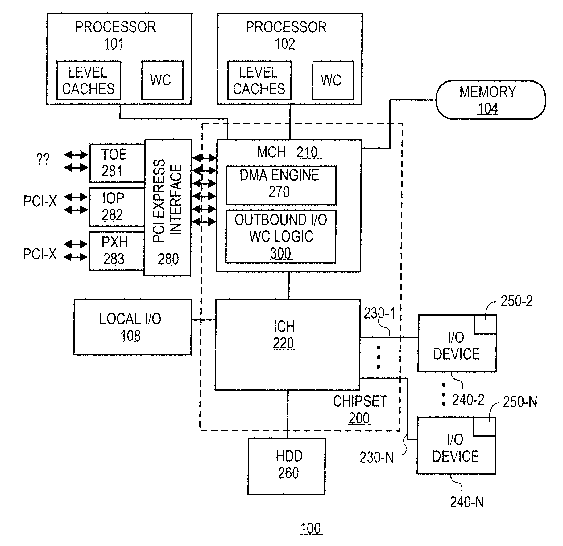
[0026]Embodiments of the present invention improve efficiency of a server chipsets used in local area network (LAN), Blade server, and / or Gigabit Ethernet I / O applications by performing on-chip write combining operations in the north bridge or memory control hub component that increases overall network throughput and bus utilization. The write combining described herein attempts to solve limitations in the prior art through the implementation of intelligent chipset hardware, specialized ordering / flush rules and interaction with a device driver that exploits these features to increase system performance. In addition, in one embodiment, the efficiency of PCI-Express (the backbone input / output (I / O) link that connects chipsets to I / O devices) is improved as result of larger outbound write packets that are dispatched to the target I / O device than what the central processing unit (CPU) is capable of generating. [The PCI Express™ bus interface protocol is defined by the PCI Express Base S...


PUM


Abstract

Methods and apparatuses for flushing write-combined data from a buffer within a memory to an input / output (I / O) device.

Description

CROSS-REFERENCE TO RELATED APPLICATIONS[0001]This application claims the benefit of U.S. application Ser. No. 10 / 977,235, entitled “Methodology and Apparatus for Implementing Write Combining,” filed on Oct. 29, 2004.FIELD OF THE INVENTION[0002]One or more embodiments of the invention relate generally to the field of integrated circuit and computer system design. More particularly, one embodiment of the invention relates to a method and apparatus for flushing write-combined data to an input / output device.BACKGROUND OF THE INVENTION[0003]The development of ever more advanced microprocessors and associated bus architectures continues at a rapid pace. Current computer systems employ advanced architectures and processors such as Pentium Pro®, Pentium II®, Pentium III®, and Pentium IV® processors, as manufactured by the Intel Corporation of Santa Clara, Calif. In such computer systems, the bus architecture is optimized for burst performance. Generally, the bus architecture may include ded...

Claims


Application Information

Patent Timeline
29 Jan 2009
Publication
US20090031058A1
IPC
G06F13/00; G06F3/00
CPC
G06F12/0831; G06F12/0879; H04L69/12; G06F13/1631; G06F12/0897
Inventors
RADHAKRISHNAN, SIVAKUMAR; BALASUBRAMANIAN, SIVA