Liquid crystal device and electronic apparatus

a liquid crystal device and electronic equipment technology, applied in non-linear optics, instruments, optics, etc., can solve the problems of difficult to achieve a sufficient aperture ratio of the pixel, difficult to achieve a high display luminance, and remarkably deteriorated light transmittance during bright displays at these locations. achieve the effect of wide viewing angle and high display luminan

Active Publication Date: 2009-09-10
JAPAN DISPLAY WEST
View PDF6 Cites 34 Cited by
  • Summary
  • Abstract
  • Description
  • Claims
  • Application Information

AI Technical Summary

Benefits of technology

[0026]According to another aspect of the invention, there is provided an electronic apparatus having the liquid crystal device according to the above aspect of the invention. According to such a configuration, it is possible to realize an electronic apparatus having a liquid crystal display unit capable of achieving a high display luminance and a wide viewing angle.

Problems solved by technology

However, since lateral electric fields are generated in various directions in portions (encircled regions indicated by symbol B in FIG. 11) of the linear electrodes 101a and 101b disposed in the vicinity of end portions thereof, the alignment of the liquid crystals is disordered, and thus, light transmittance during bright display is remarkably deteriorated at these locations.
Therefore, in this configuration, the area capable of substantially contributing to display is decreased, and thus, it is difficult to obtain a sufficient aperture ratio of the pixel and to achieve a high display luminance.
Consequently, there is a problem that it is difficult to achieve a high display luminance.
When the slits are connected with each other across both sides of the bent portions, there is a fear that it may cause problems that display defects resulting from an alignment disorder (disclination) of liquid crystals at the bent portions may spread or that the display defects may be unstably transferred to other positions upon application of an external force to the liquid crystal device.
According to the configuration of the above aspect of the invention, although it is possible to provide a high aperture ratio, there is a fear that when a larger part of the outer border of the second electrode is located in close proximity of the data line, due to the influence of an electric field generated between the data line and the second electrode, the alignment of the liquid crystal molecules between them is disordered, thus leading to display defects.

Method used


Image

  • Liquid crystal device and electronic apparatus
  • Liquid crystal device and electronic apparatus
  • Liquid crystal device and electronic apparatus

Examples


first embodiment

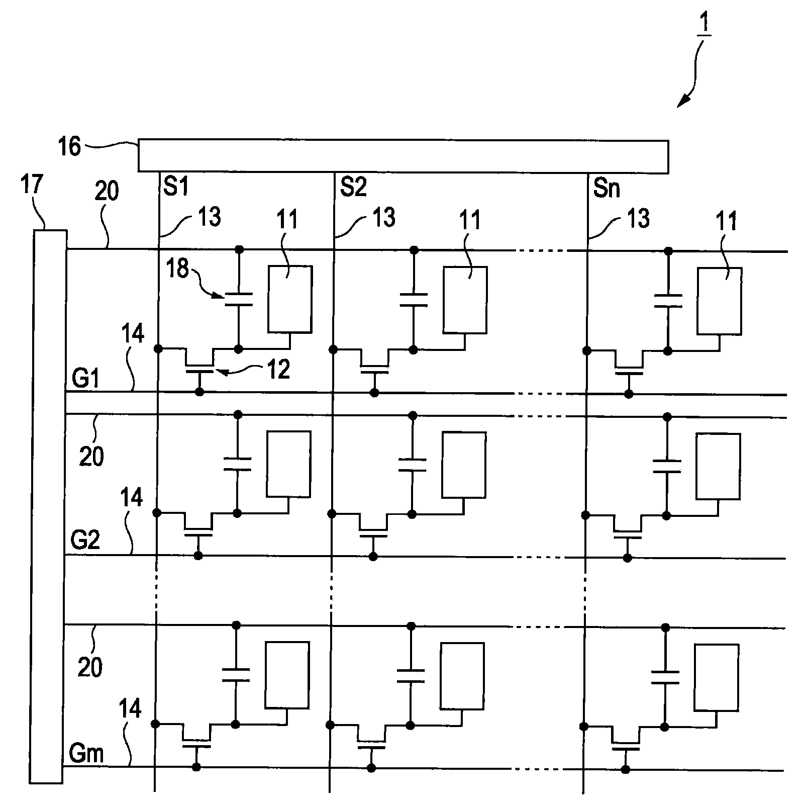
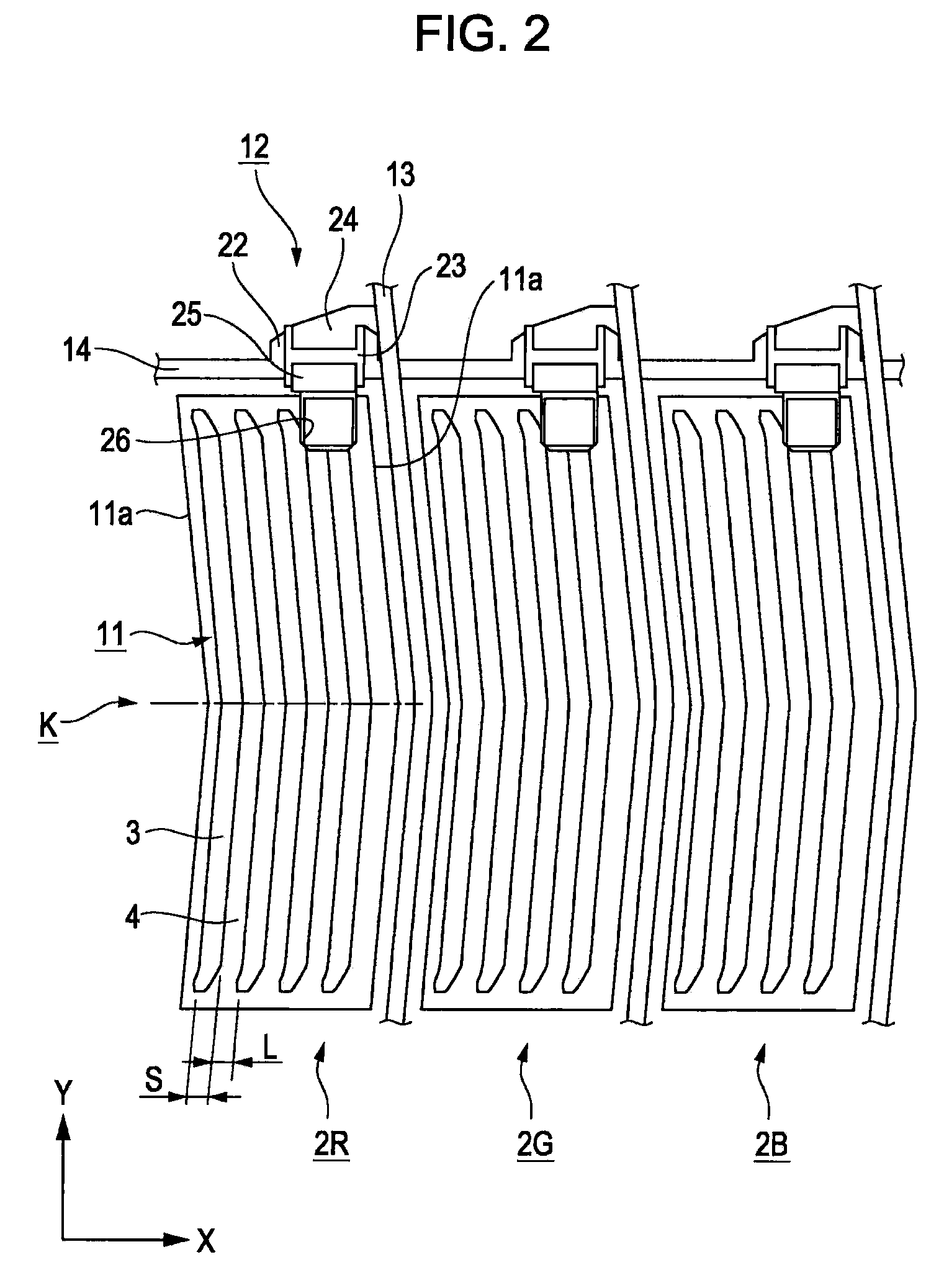
[0039]A liquid crystal device according to a first embodiment of the invention will be described herein below with reference to FIGS. 1 to 4. The liquid crystal device according to this embodiment is an example of a FFS mode color liquid crystal display device. FIG. 1 is an equivalent circuit diagram of the liquid crystal device according to this embodiment. FIG. 2 is a plan view illustrating a configuration of one pixel of the liquid crystal device. FIG. 3 is a cross-sectional view illustrating the configuration of one pixel of the liquid crystal device. In the drawings below, individual members are appropriately depicted with different reduced scales in order to make them large enough to be recognized on the drawings.

[0040]A liquid crystal device 1 according to this embodiment is a color liquid crystal display device in which one pixel is configured by three sub-pixels capable of outputting color light of red (R), green (G) and blue (B). Here, a display region which serves the min...

second embodiment

[0055]A liquid crystal device according to a second embodiment of the invention will be described herein below with reference to FIG. 4. A basic configuration of the liquid crystal device according to this embodiment is the same as that of the first embodiment, except that the pixel electrode is configured differently from that of the first embodiment. FIG. 4 is a plan view illustrating the configuration of one pixel of the liquid crystal device according to this embodiment. In FIG. 4, the same constituent elements as those of FIG. 2 used in the first embodiment will be denoted by the same reference numerals and the detailed descriptions thereof will be omitted.

[0056]In the first embodiment, the slits 3 formed within the pixel electrode 11 were formed to be connected with each other across both sides of the bent portions K. To the contrary, in the liquid crystal device according to this embodiment, as illustrated in FIG. 4, connection portions 55 are formed between the bent portions...

third embodiment

[0058]A liquid crystal device according to a third embodiment of the invention will be described herein below with reference to FIG. 5. A basic configuration of the liquid crystal device according to this embodiment is the same as that of the first and second embodiments, except that the pixel electrode is configured differently from that of the first and second embodiments. FIG. 5 is a plan view illustrating the configuration of one pixel of the liquid crystal device according to this embodiment. In FIG. 5, the same constituent elements as those of FIG. 2 used in the first embodiment will be denoted by the same reference numerals and the detailed descriptions thereof will be omitted.

[0059]In the first and second embodiments, the width L of the linear electrodes and the width S of the slits were constant within the pixel electrode. To the contrary, in the liquid crystal device according to this embodiment, as illustrated in FIG. 5, the width of the linear electrodes and the width of...


PUM

PropertyMeasurementUnit
inclination angleaaaaaaaaaa
angleaaaaaaaaaa

Abstract

A liquid crystal device is provided which includes: a first substrate and a second substrate that are disposed to face each other; a liquid crystal layer that is sandwiched between the first substrate and the second substrate; a first electrode that is provided on the liquid crystal layer side of the first substrate; an insulating layer that is provided on the liquid crystal layer side of the first electrode; and a second electrode that is provided on the liquid crystal layer side of the insulating layer, in which the first substrate has formed thereon a plurality of data lines and a plurality of scan lines which intersect each other; sub-pixels are formed at regions surrounded by the data lines and the scan lines; the second electrode has a plurality of linear electrodes that is disposed with a gap therebetween; each of the plurality of linear electrodes extends in a long-axis direction of the sub-pixels and has at least one bent portion; the bent portion has such a shape that both sides thereof are inclined in opposite directions with respect to the long-axis direction of the sub-pixels; and the data lines or the scan lines are bent in an extending direction of the linear electrodes having the bent portion.

Description

CROSS REFERENCES TO RELATED APPLICATIONS[0001]The present invention contains subject matter related to Japanese Patent Application No. 2009-009615 filed in the Japanese Patent Office on Jan. 20, 2009, the entire contents of which are incorporated herein by reference.BACKGROUND[0002]1. Technical Field[0003]The invention relates to a liquid crystal device and an electronic apparatus.[0004]2. Related Art[0005]Hitherto, as one means for achieving a wide viewing angle of an liquid crystal device, there has been used a mode in which an electric field is applied to a liquid crystal layer in a direction of a substrate plane to thereby control alignment of liquid crystal molecules (such a mode will be referred to as a lateral electric field mode), and an IPS (In-Plane Switching) mode and an FFS (Fringe-Field Switching) mode have been known as such a lateral electric field mode. In a lateral electric field mode liquid crystal device, a pixel electrode and a common electrode are typically form...

Claims


Application Information

Patent Timeline
Patent Type & Authority Applications(United States)
IPC IPC(8): G02F1/1343
CPCG02F1/134363G02F2001/134372G02F2201/40G02F1/1368G02F1/133512G02F1/13439G02F1/133345G02F1/134372G02F1/134345
Inventor ATARASHIYA, TAKAOKURASAWA, HAYATO
Owner JAPAN DISPLAY WEST
Why Eureka
Try Eureka