Eureka AIR delivers breakthrough ideas for toughest innovation challenges, trusted by R&D personnel around the world.

Resistive random access memory

Inactive Publication Date: 2009-12-10
SAMSUNG ELECTRONICS CO LTD
View PDF2 Cites 77 Cited by
  • Summary
  • Abstract
  • Description
  • Claims
  • Application Information

AI Technical Summary

Benefits of technology

[0014]At least one other example embodiment provides a multi-layer RRAM structure including a plurality of RRAMs arranged in an array. Each RRAM may include a switch region and a memory resistor. The switch region may include an intermediate layer including an electrolyte, and a nano bridge formed on the intermediate layer. The memory resistor may have variable resistance properties.
[0015]At least one other example embodiment provides a multi-layer

Problems solved by technology

However, conventional DRAMs are volatile memories, which do not retain data when power is shut off.
Conventional flash memories, however, cannot be as highly integrated, and have a relatively low operating speed when compared with conventional DRAMs.

Method used


Image

  • Resistive random access memory
  • Resistive random access memory
  • Resistive random access memory

Examples


Embodiment Construction

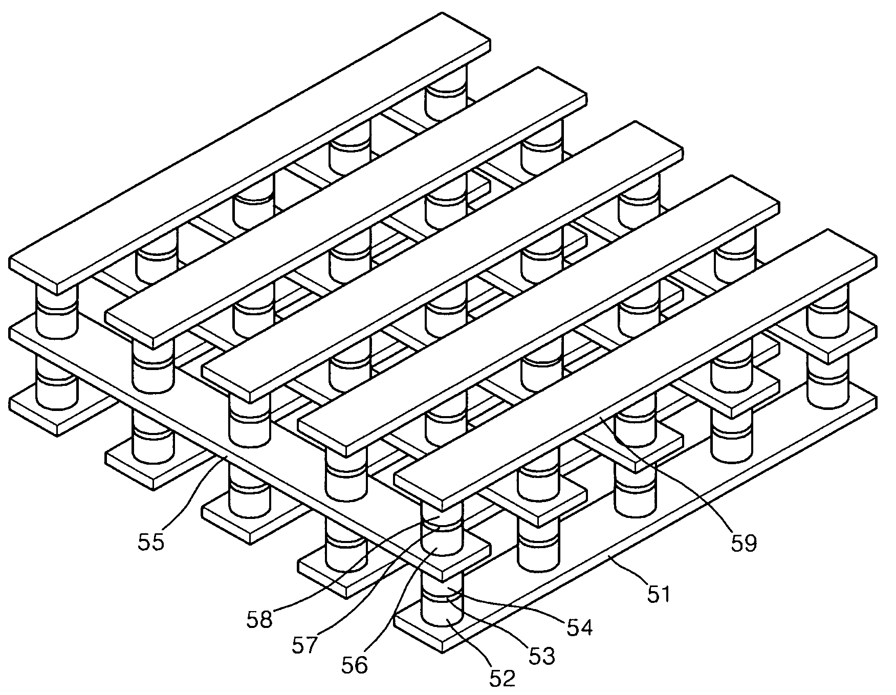
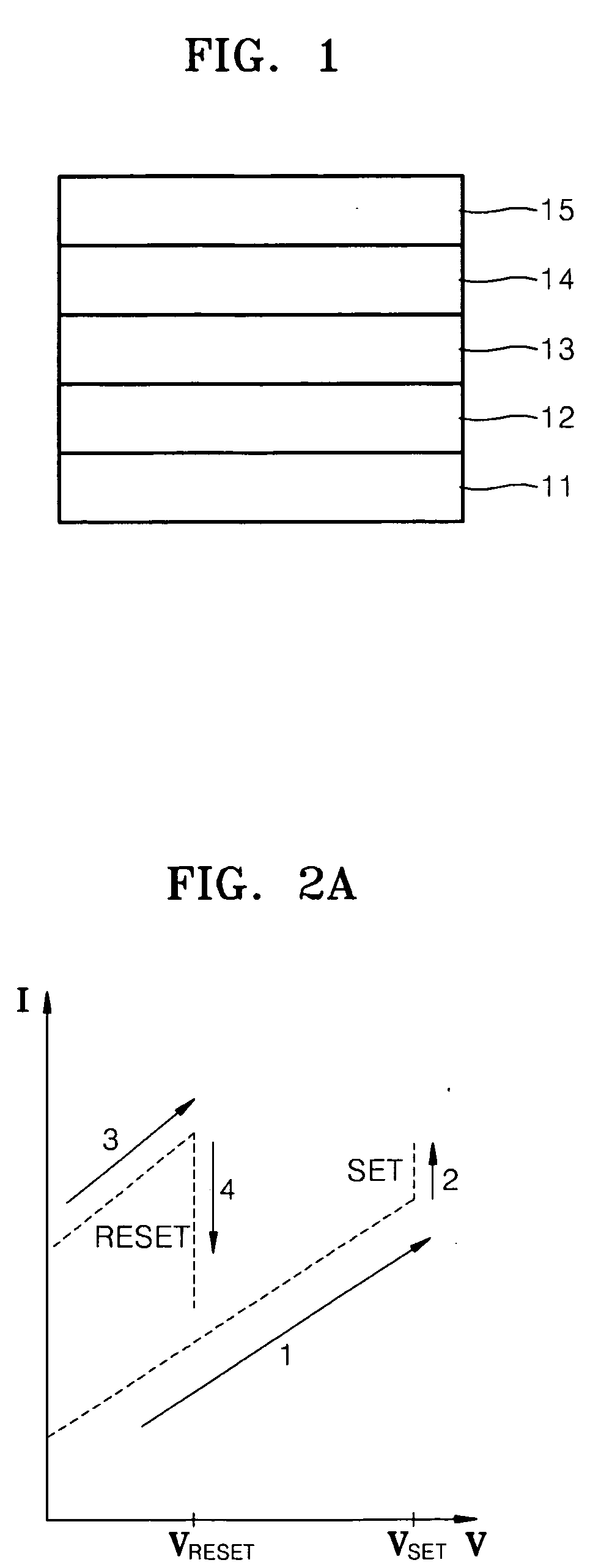
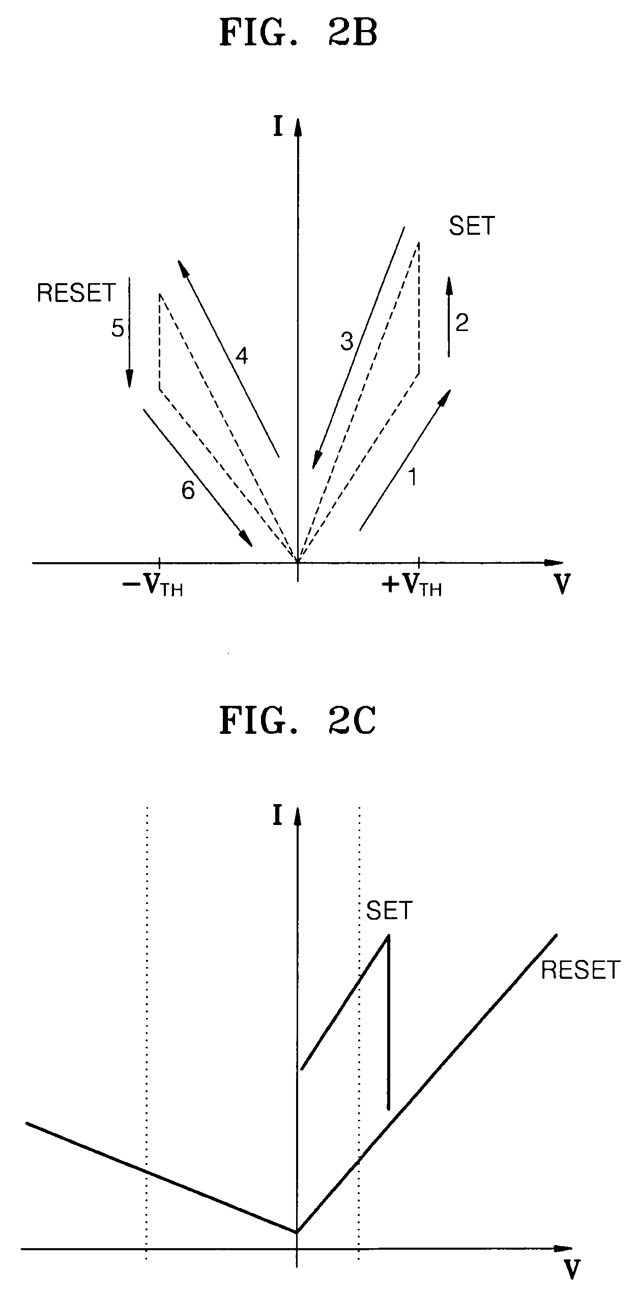
[0026]Reference will now be made in detail to example embodiments which are illustrated in the accompanying drawings, wherein like reference numerals refer to the like elements throughout. In this regard, example embodiments may have different forms and should not be construed as being limited to the descriptions set forth herein. Accordingly, the example embodiments are merely described below, by referring to the figures, to explain aspects of the present description. In the drawings, the thicknesses of layers and regions are exaggerated for clarity.

[0027]Detailed example embodiments are disclosed herein. However, specific structural and functional details disclosed herein are merely representative for purposes of describing example embodiments. The present inventive concept may, however, may be embodied in many alternate forms and should not be construed as limited to only the example embodiments set forth herein.

[0028]Accordingly, while example embodiments are capable of various ...


PUM


Abstract

A resistive random access memory (RRAM) includes a switch region formed of a material having bi-polar properties; and a memory resistor formed of a material having uni-polar properties. The RRAM further includes a lower electrode formed below the switch region; an upper electrode formed on the memory resistor; and an intermediate electrode formed between the switch region and the memory resistor.

Description

CROSS-REFERENCE TO RELATED APPLICATION[0001]This application claims priority under 35 U.S.C. §119 to Korean Patent Application No. 10-2008-0052666, filed on Jun. 4, 2008, in the Korean Intellectual Property Office, the disclosure of which is incorporated herein in its entirety by reference.BACKGROUND[0002]1. Field[0003]One or more example embodiments relate to memories such as resistive random access memories (RRAMs) including a switch structure.[0004]2. Description of the Related Art[0005]A conventional semiconductor memory array includes many memory cells connected through a given or predetermined circuit structure. A conventional dynamic random access memory (DRAM), which is a representative example of a semiconductor memory array, includes a single switch and a single capacitor. A conventional DRAM is a highly integrated, relatively rapid memory device. However, conventional DRAMs are volatile memories, which do not retain data when power is shut off. On the other hand, a nonvol...

Claims


Application Information

Patent Timeline
IPC IPC(8): H01L29/12H01L29/00
CPCH01L45/04H01L45/085H01L45/1233H01L45/142H01L27/2481H01L45/146H01L45/147H01L27/2409H01L45/143H10B63/20H10B63/84H10N70/245H10N70/20H10N70/826H10N70/8822H10N70/8825H10N70/8833H10N70/8836G11C13/0004
Inventor LEE, CHANGBUMPARK, YOUNGSOOLEE, MYOUNGJAEKANG, BOSOOAHN, SEUNGEONKIM, KIHWAN
Owner SAMSUNG ELECTRONICS CO LTD
Why Eureka
Eureka Blog
Learn More