Solid-state imaging device and imaging apparatus
- Summary
- Abstract
- Description
- Claims
- Application Information
AI Technical Summary
Benefits of technology
Problems solved by technology
Method used
Image

Examples
Embodiment Construction
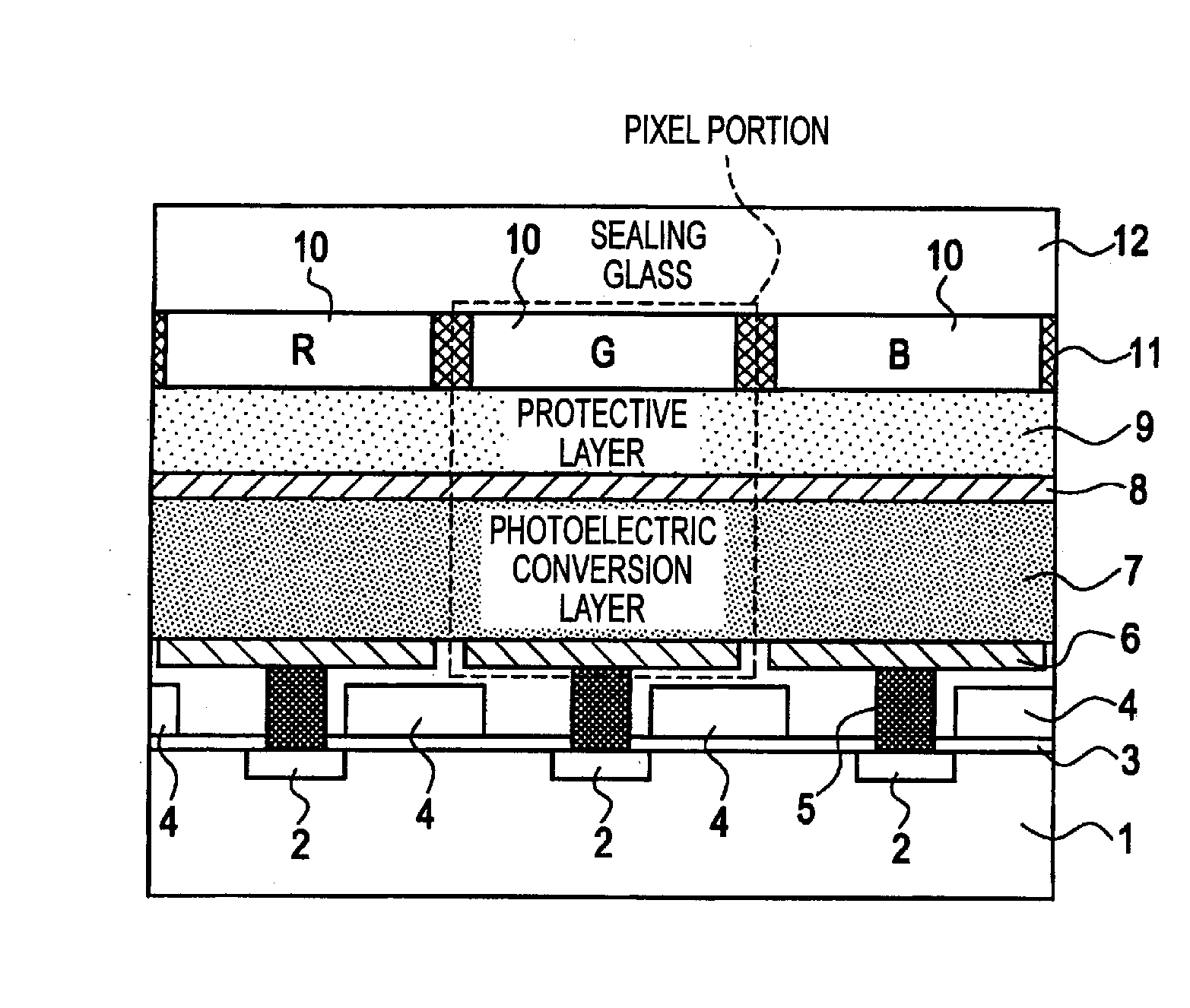
[0028]A solid-state imaging device according to an embodiment of the present invention will be hereinafter described with reference to the drawings. This solid-state imaging device is for use in imaging apparatus such as digital cameras and digital video cameras.
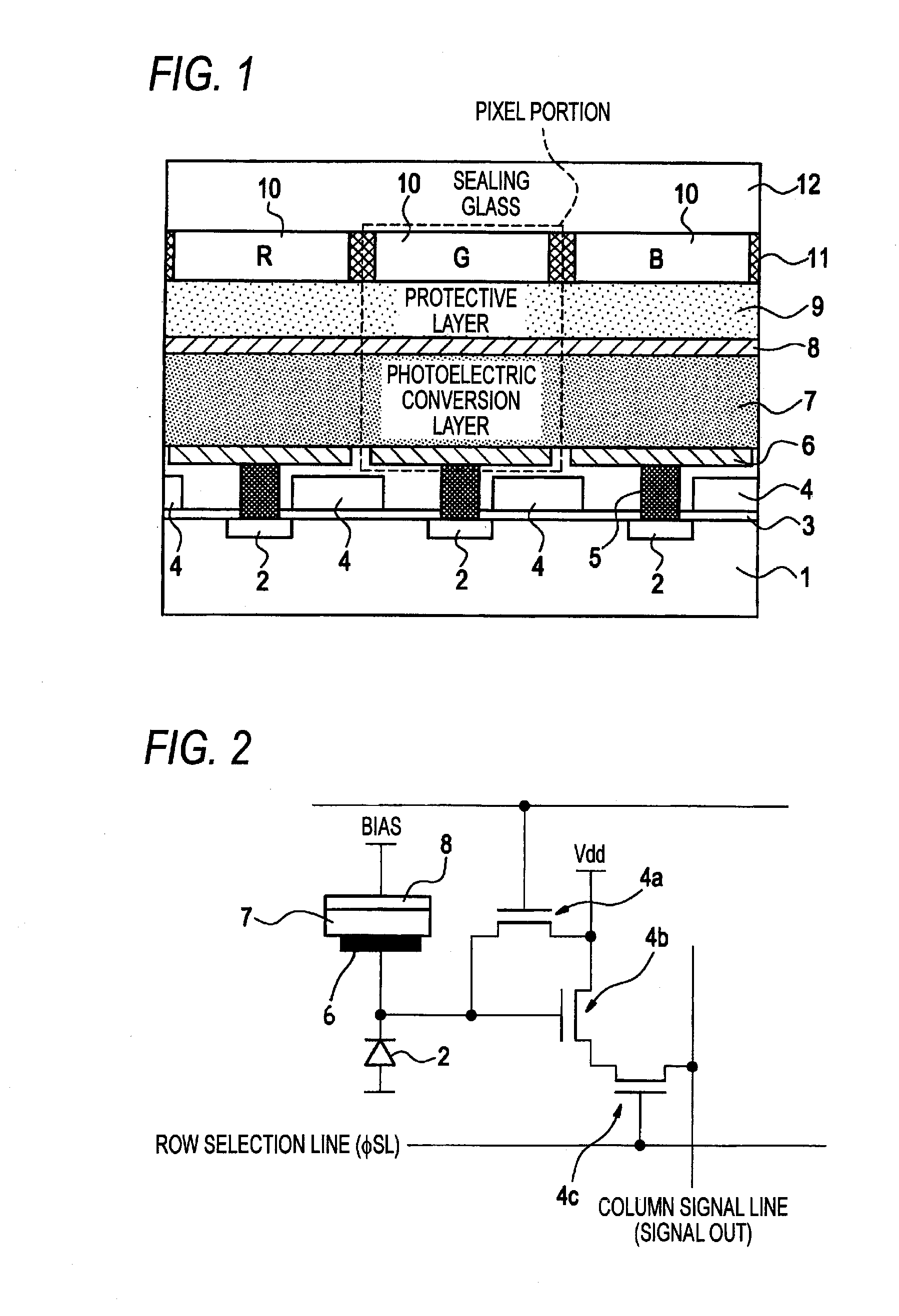
[0029]FIG. 1 is a schematic sectional view showing a general configuration of the solid-state imaging device according to the embodiment of the invention. In the solid-state imaging device of FIG. 1, many pixel portions are disposed over a p-type silicon substrate 1 (an example of the term “substrate” as used in the claims) so as to be arranged two-dimensionally (e.g., in square matrix) or one-dimensionally. For example, the pixel portions are rectangular in shape. FIG. 1 includes a cross section of three pixel portions that are arranged in a prescribed direction.
[0030]Each pixel portion is provided with a photoelectric conversion portion including a lower electrode 6 disposed over the p-type silicon substrate 1, an upper el...
PUM
 Abstract
Description
Claims
Application Information