Check patentability & draft patents in minutes with Patsnap Eureka AI!

Solid-state imaging device and imaging apparatus having light-preventing partitions

a technology of solid-state imaging and imaging apparatus, which is applied in the direction of radioation control devices, television system scanning details, television systems, etc., can solve the problems of color contamination and color contamination that are not negligibl

Active Publication Date: 2012-08-07
FUJIFILM CORP
View PDF4 Cites 8 Cited by
  • Summary
  • Abstract
  • Description
  • Claims
  • Application Information

AI Technical Summary

Benefits of technology

The present invention provides a solid-state imaging device and an imaging apparatus that can suppress color contamination even in the case of small pixel portions. The device includes partitions that prevent light from leaking into adjacent pixel portions, which can be made of a light absorbing or reflecting material or air layers. The device also includes a photoelectric conversion layer that absorbs visible light and generates signal charges, and color filters that transmit light components in different wavelength ranges. The device can be used in an imaging apparatus.

Problems solved by technology

However, if there exists a certain distance between the photoelectric conversion layer and the mosaic color filters, light that is incident on each pixel portion obliquely may leak into adjacent pixel portions to cause color contamination.
However, the problem of color contamination will not be negligible when the degree of miniaturization of the pixel portions is increased and each pixel portion comes to measure less than 2 μm, in particular, around 1 μm, in the future.

Method used


Image

  • Solid-state imaging device and imaging apparatus having light-preventing partitions
  • Solid-state imaging device and imaging apparatus having light-preventing partitions
  • Solid-state imaging device and imaging apparatus having light-preventing partitions

Examples


Embodiment Construction

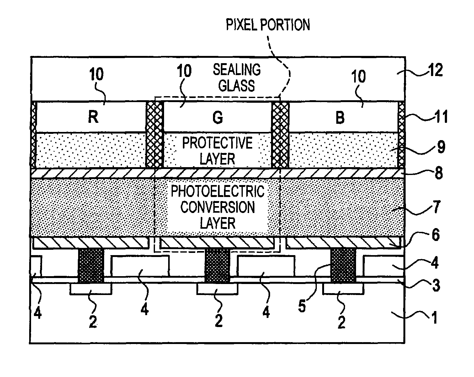
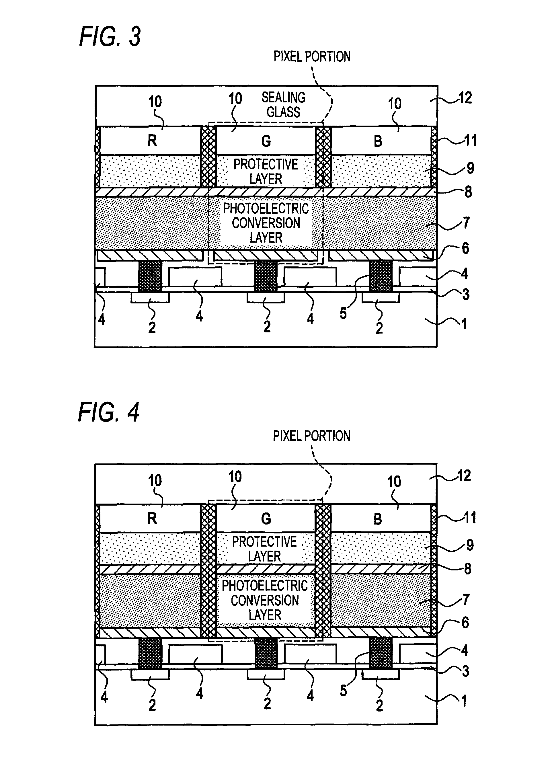
[0028]A solid-state imaging device according to an embodiment of the present invention will be hereinafter described with reference to the drawings. This solid-state imaging device is for use in imaging apparatus such as digital cameras and digital video cameras.

[0029]FIG. 1 is a schematic sectional view showing a general configuration of the solid-state imaging device according to the embodiment of the invention. In the solid-state imaging device of FIG. 1, many pixel portions are disposed over a p-type silicon substrate 1 (an example of the term “substrate” as used in the claims) so as to be arranged two-dimensionally (e.g., in square matrix) or one-dimensionally. For example, the pixel portions are rectangular in shape. FIG. 1 includes a cross section of three pixel portions that are arranged in a prescribed direction.

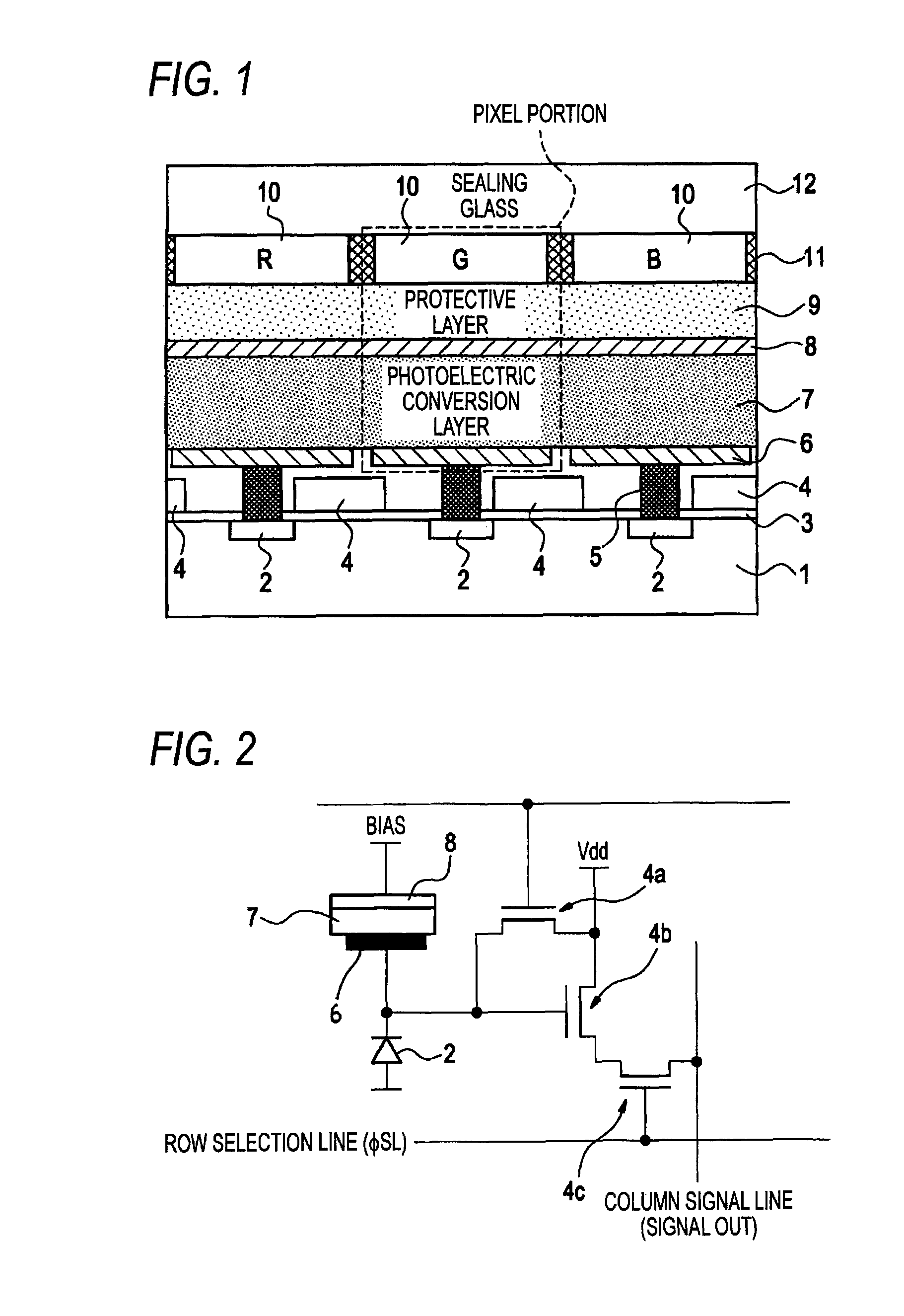
[0030]Each pixel portion is provided with a photoelectric conversion portion including a lower electrode 6 disposed over the p-type silicon substrate 1, an upper el...


PUM


Abstract

A solid-state imaging device includes a substrate and a plurality of pixel portions arranged over the substrate, each of the pixel portions includes a photoelectric conversion portion provided over the substrate and a color filter provided over the photoelectric conversion portion, and the solid-state imaging device includes partitions for preventing light that is incident on the color filter of each pixel portion from entering adjacent pixel portions.

Description

CROSS-REFERENCE TO RELATED APPLICATIONS[0001]This application claims the benefit of Japanese Patent Application JP2008-233316, filed Sep. 11, 2008, the entire content of which is hereby incorporated by reference, the same as if set forth at length.FIELD OF THE INVENTION[0002]The present invention relates to a solid-state imaging device having many pixel portions arranged over a substrate and an imaging apparatus having such a solid-state imaging device.BACKGROUND OF THE INVENTION[0003]Stacked color imaging devices are known which have a layer of an organic photoelectric conversion material or an inorganic photoelectric conversion material such as amorphous silicon or a compound semiconductor and mosaic color filters disposed over the photoelectric conversion layer (refer to JP-A-2005-347475 and Hitachi, Ltd., “Single-plate Color Solid-state Imaging Device Using Amorphous Si,” ITEJ Technical Report TEBS76-1-1). The photoelectric conversion layer absorbs visible light and generates si...

Claims


Application Information

Patent Timeline
Patent Type & Authority Patents(United States)
IPC IPC(8): H04N3/14H04N5/335H01L27/14H01L27/146H04N25/00
CPCH01L27/14623H01L27/14625H01L27/14632H04N9/04H04N9/045H04N9/07H01L27/14685H01L27/14621H01L27/14627H04N23/10H04N23/12H04N25/76
Inventor INUIYA, MASAFUMI
Owner FUJIFILM CORP
Features
  • R&D
  • Intellectual Property
  • Life Sciences
  • Materials
  • Tech Scout
  • Unparalleled Data Quality
  • Higher Quality Content
  • 60% Fewer Hallucinations
Learn More