Embedded circuit substrate and manufacturing method thereof

a technology of embedded circuit substrate and manufacturing method, which is applied in the direction of printed circuit aspects, non-metallic protective coating applications, conductive pattern formation, etc., can solve the problem that the conventional structure and manufacturing process of embedded circuit substrate are no longer sufficient for us

Active Publication Date: 2010-06-10
ADVANCED SEMICON ENG INC
View PDF4 Cites 68 Cited by
  • Summary
  • Abstract
  • Description
  • Claims
  • Application Information

AI Technical Summary

Problems solved by technology

However, with the improvement of integrity and flatness, the conventional structur

Method used


Image

  • Embedded circuit substrate and manufacturing method thereof
  • Embedded circuit substrate and manufacturing method thereof
  • Embedded circuit substrate and manufacturing method thereof

Examples


Embodiment Construction

[0015]Reference will now be made in detail to the present preferred embodiments of the invention, examples of which are illustrated in the accompanying drawings. Wherever possible, the same reference numbers are used in the drawings and the description to refer to the same or like parts.

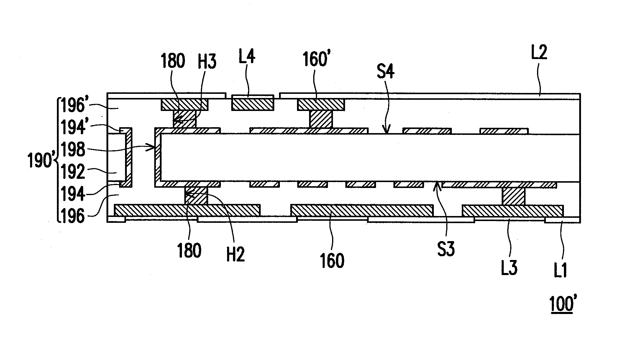
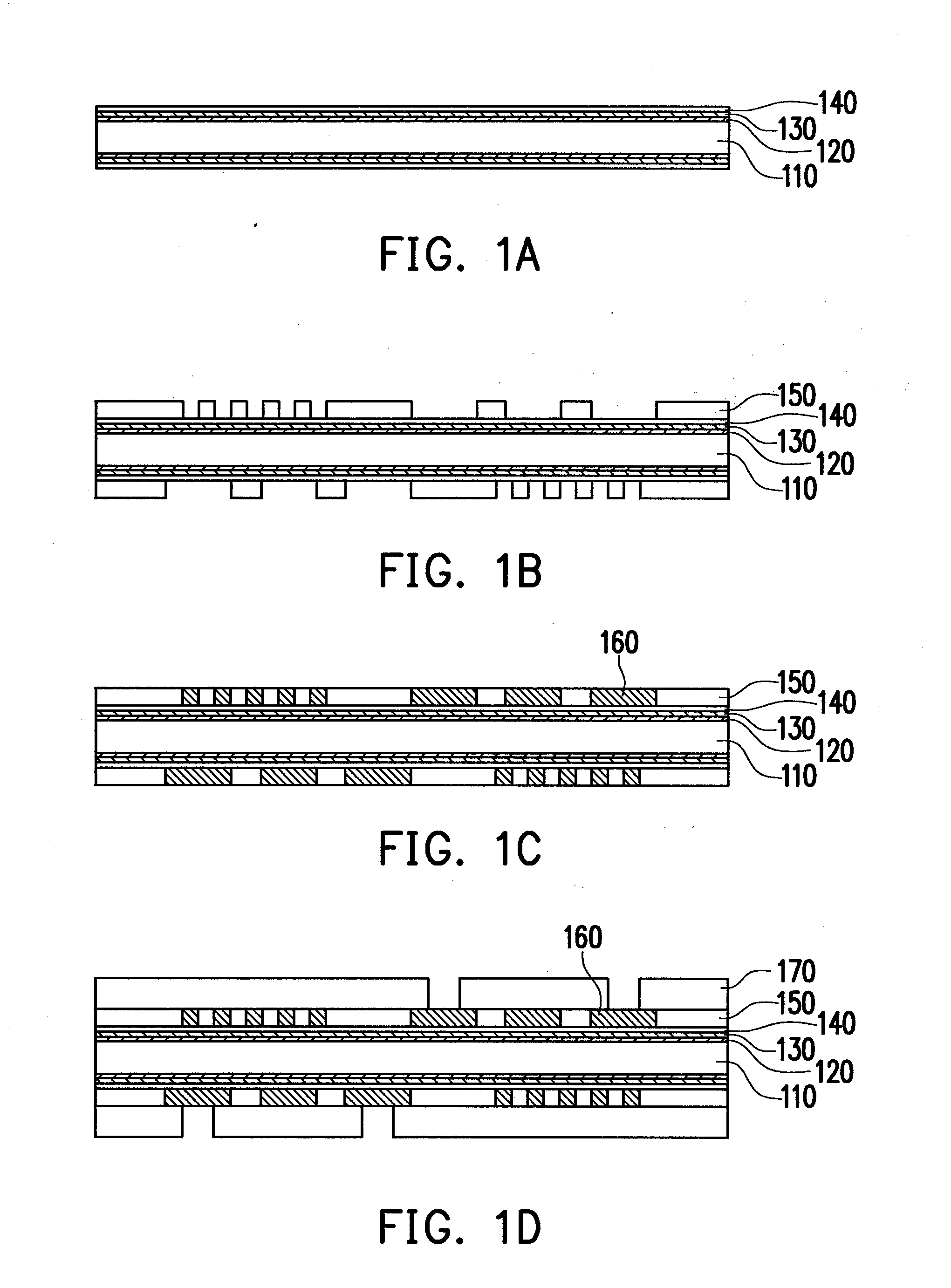
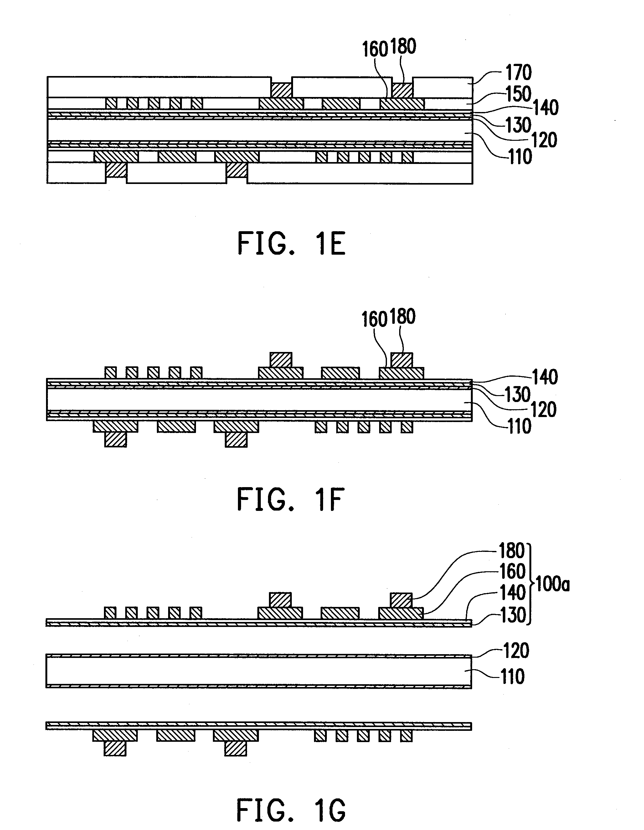
[0016]FIGS. 1A to 1L are cross-sectional views showing a manufacturing process according to an embodiment of the present invention. First, referring to FIG. 1A, a sacrifice layer 110, two third metal layers 120 disposed on two opposite surfaces of the sacrifice layer 110 and two first metal layers 130 disposed on the two third metal layers 120 are provided. Each third metal layer 120 is located between the sacrifice layer 110 and the corresponding first metal layer 130. In this embodiment, a first etching stopping layer 140 can be further formed on each first metal layer 130.

[0017]Next, referring to FIG. 1B, a first mask layer 150 is formed on each first etching stopping layer 140, wherein each first...


PUM

PropertyMeasurementUnit
Electrical conductoraaaaaaaaaa

Abstract

An embedded circuit substrate comprising: a core structure having a first surface and a second surface opposite to each other; a first patterned conductive layer disposed on the first surface and embedded in the core structure; a second patterned conductive layer disposed on the second surface and embedded in the core structure; and a plurality of conductive blocks disposed in the core structure for conducting the first patterned conductive layer and the second patterned conductive layer is provided. Furthermore, a manufacturing method of an embedded circuit substrate is also provided.

Description

CROSS-REFERENCE TO RELATED APPLICATION[0001]This application claims the priority benefit of Taiwan application serial no. 97147880, filed on Dec. 9, 2008. The entirety of the above-mentioned patent application is hereby incorporated by reference herein and made a part of this specification.BACKGROUND OF THE INVENTION[0002]1. Field of the Invention[0003]The present invention generally relates to a circuit substrate and a manufacturing method thereof. More particularly, the present invention relates to an embedded circuit substrate and a manufacturing method thereof.[0004]2. Description of Related Art[0005]In semiconductor package, circuit substrate is one of the packaging devices in common use. The circuit substrate is constituted by patterned conductive layers and dielectric layers interlaced to each other, wherein two circuit layer are electrically connected through conductive vias. However, with the improvement of integrity and flatness, the conventional structure and manufacturin...

Claims


Application Information

Patent Timeline
IPC IPC(8): H05K1/11H05K3/10
CPCH05K3/0097H05K3/205H05K3/28H05K3/4602H05K3/462H05K3/4647Y10T29/49128H05K2201/09563H05K2203/063H05K2203/0733H05K2203/1536Y10T29/49126Y10T29/49155H05K3/4658
Inventor WANG, CHIEN-HAOLEE, MING-CHIANG
Owner ADVANCED SEMICON ENG INC
Why Eureka
Try Eureka