Circuit board and electronic device with the same

a technology of circuit boards and electronic devices, applied in the direction of printed circuit aspects, electrical apparatus construction details, electrical apparatus casings/cabinets/drawers, etc., can solve the problems of lateral displacement of abnormal noise between circuit boards, and achieve the effect of increasing static friction force (or coefficient), preventing or suppressing abnormal noise, and high hardness

Active Publication Date: 2010-06-10
KK TOKAI RIKA DENKI SEISAKUSHO
View PDF18 Cites 6 Cited by
  • Summary
  • Abstract
  • Description
  • Claims
  • Application Information

AI Technical Summary

Benefits of technology

[0027]According one embodiment of the invention, a circuit board is constructed such that, by being fastened by screws, the front surface of a boss-like fixing part contacts strong with a printed portion (e.g., silk-screen prints) that includes a lattice printed portion and a ring printed portion formed on the circuit board corresponding to the boss-like fixing part. Here, the housing is formed of a resin such as ABS and the silk-screen prints are formed of a high hardness epoxy ink. Therefore, the printed portion, especially, the ink part of the lattice printed portion bites into the contact face of the boss-like fixing part to increase the static friction force (or coefficient) for preventing or suppressing abnormal noise upon the lateral displacement between the circuit board and the surface of the housing due to temperature change.

Problems solved by technology

However, the circuit board in JP-A-2008-258501 is fixed to the surface of the housing by the fastening power of the screw, so that abnormal noise may arise upon the lateral displacement between the circuit board and the surface of the housing when the circuit board contracts due to temperature change in the interior of the electronic device or the housing.

Method used


Image

  • Circuit board and electronic device with the same
  • Circuit board and electronic device with the same
  • Circuit board and electronic device with the same

Examples


Embodiment Construction

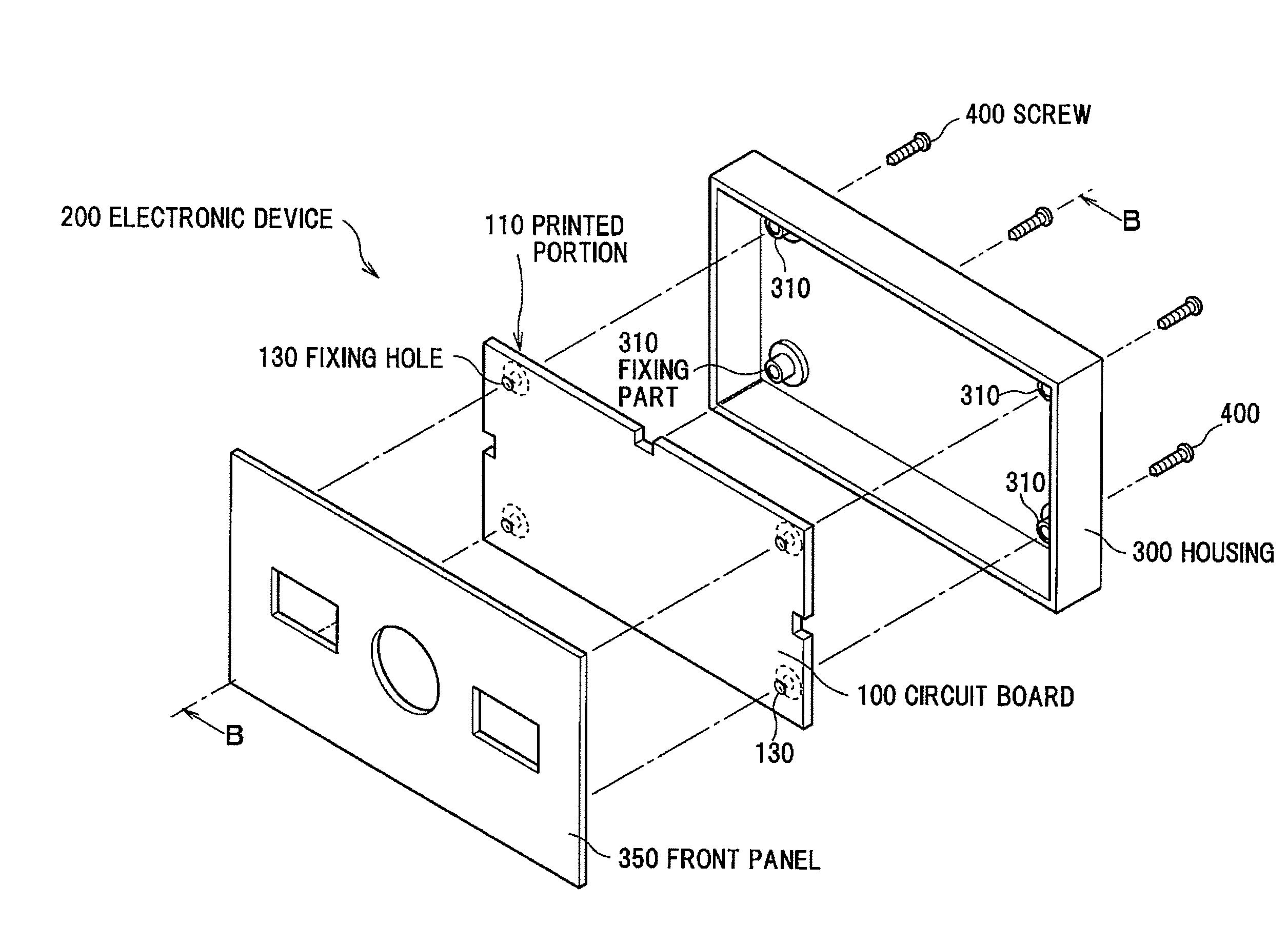
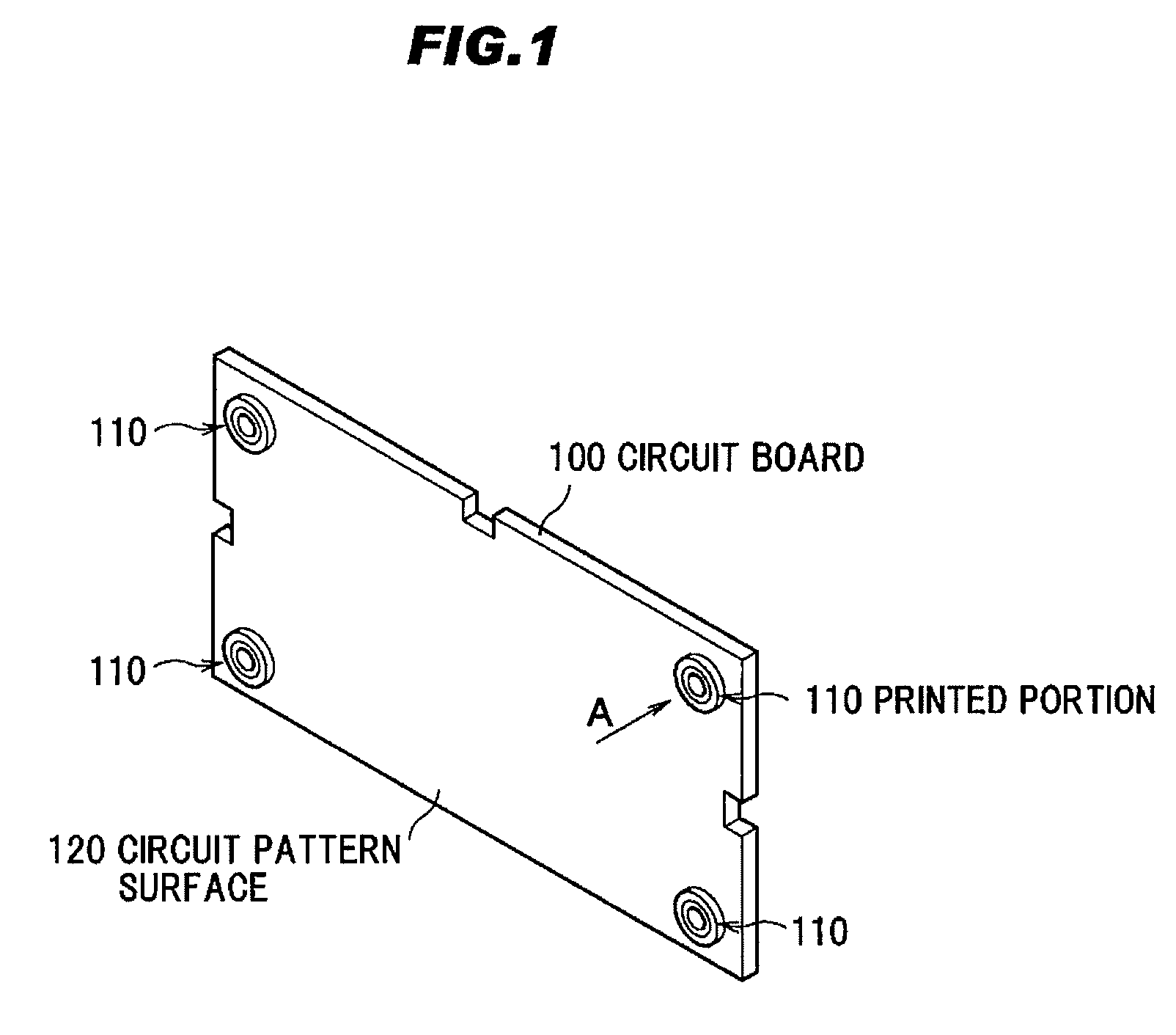
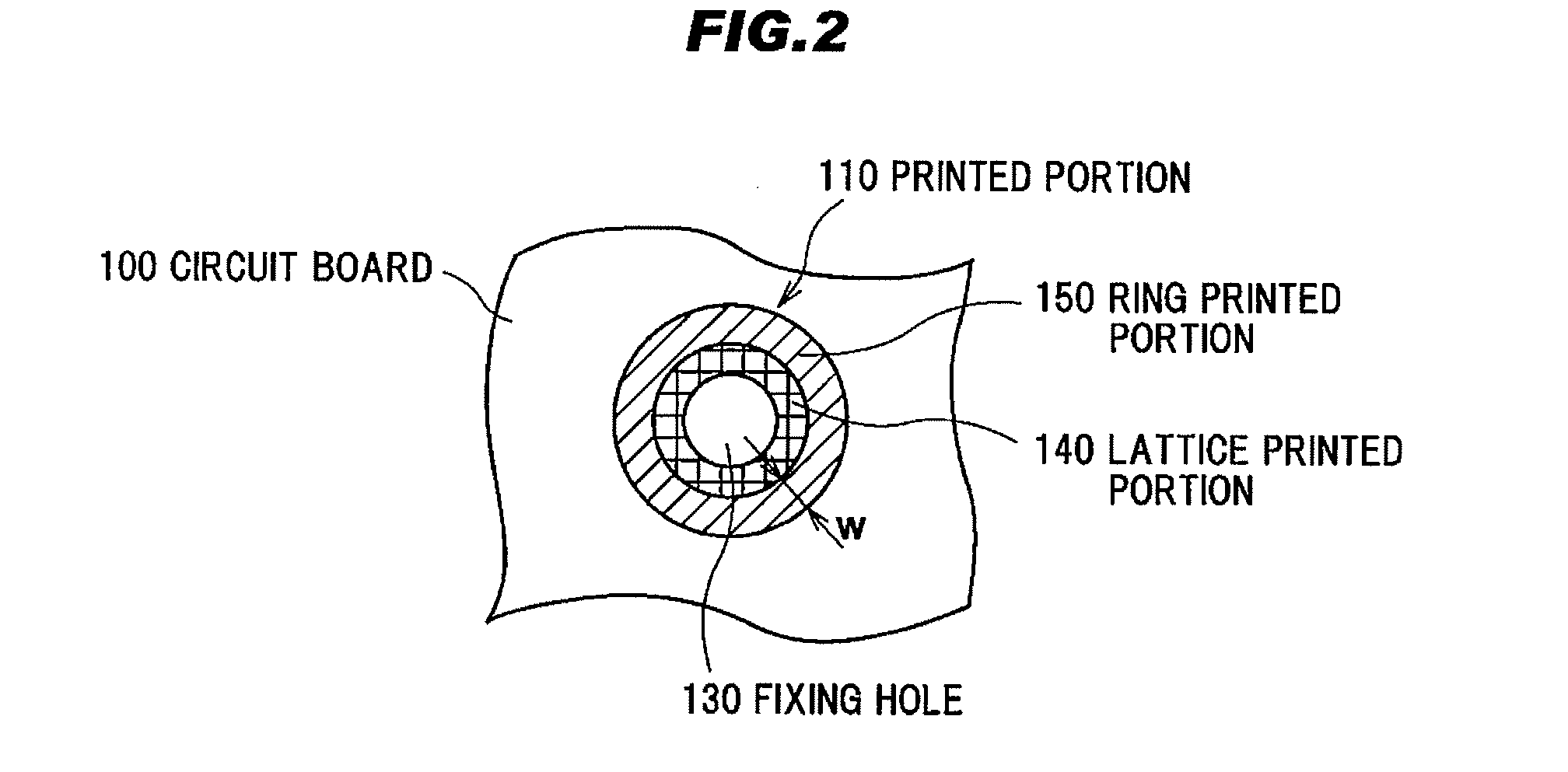
[0034]The preferred embodiments according to the invention will be explained below referring to the drawings. FIG. 1 is a perspective view showing a circuit board in a preferred embodiment according to the invention. FIG. 2 is an enlarged plan view showing a printed portion which is viewed in a direction A in FIG. 1. FIG. 3 is an exploded perspective view showing an electronic device with the circuit board housed therein. FIG. 4 is a cross sectional view cut along a line B-B in an assembled state of the electronic device in FIG. 3. FIG. 5 is a cross sectional view cut along a line C-C in FIG. 4.

[0035]The circuit board 100 of the embodiment is constructed such that it is fixed to a housing 300 as a first housing with a boss-like fixing part 310 by being fastened by screws 400 as a fixing tool, and provided with a printed portion 110 in a region where it contacts with the housing 300.

[0036]As shown in FIG. 1, a circuit pattern surface 120 with a circuit pattern formed thereon is provi...


PUM


Abstract

A circuit board is fixed to a housing including a boss-like fixing part by being fastened by a fixing tool. The circuit board includes a printed portion formed in a region that the circuit board contacts with the housing. The printed portion includes a lattice printed portion formed by silk screening on a periphery of a fixing hole through which the fixing tool is inserted, and a ring printed portion formed by silk screening on a periphery of the lattice printed portion. The lattice printed portion includes a non-printed region, and the ring printed portion includes no non-printed region.

Description

[0001]The present application is based on Japanese patent application No. 2008-311136 filed on Dec. 5, 2008, the entire contents of which are incorporated herein by reference.BACKGROUND OF THE INVENTION[0002]1. Field of the Invention[0003]This invention relates to a circuit board and an electronic device equipped with the circuit board.[0004]2. Description of the Related Art[0005]Conventionally electronic devices are constructed such that a circuit board with an electronic parts mounted thereon is enclosed in a housing, and the circuit board is fixed to a part of the housing by screws passing through a fixing hole formed in the circuit board (See, e.g., JP-A-2008-258501). The circuit board is provided with a conductive pattern on the periphery of the fixing hole. Thereby, when the circuit board is fixed to the housing by screws, it can be electrically connected to the housing through the conductive pattern.[0006]On the other hand, silk-screen prints are generally provided on the sur...

Claims


Application Information

Patent Timeline
Patent Type & Authority Applications(United States)
IPC IPC(8): H05K5/00
CPCH05K1/02H05K7/142H05K9/0039H05K2201/09063H05K2201/09909H05K2201/10409H05K2201/10598
Inventor UEMURA, TSUNEHITOUENO, HIROSHI
Owner KK TOKAI RIKA DENKI SEISAKUSHO
Why Eureka
Try Eureka