Touch-sensing display apparatus and fabricating method thereof
a display apparatus and touch-sensing technology, applied in the manufacture of electrode systems, electric discharge tubes/lamps, instruments, etc., can solve the problems of oled decay and certain thickness of oled touch-sensing display apparatuses
- Summary
- Abstract
- Description
- Claims
- Application Information
AI Technical Summary
Benefits of technology
Problems solved by technology
Method used
Image
Examples
Embodiment Construction
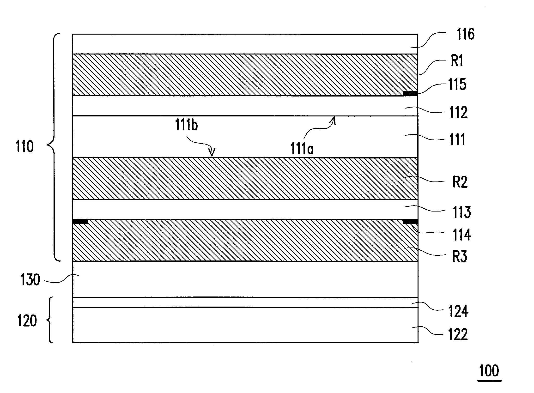
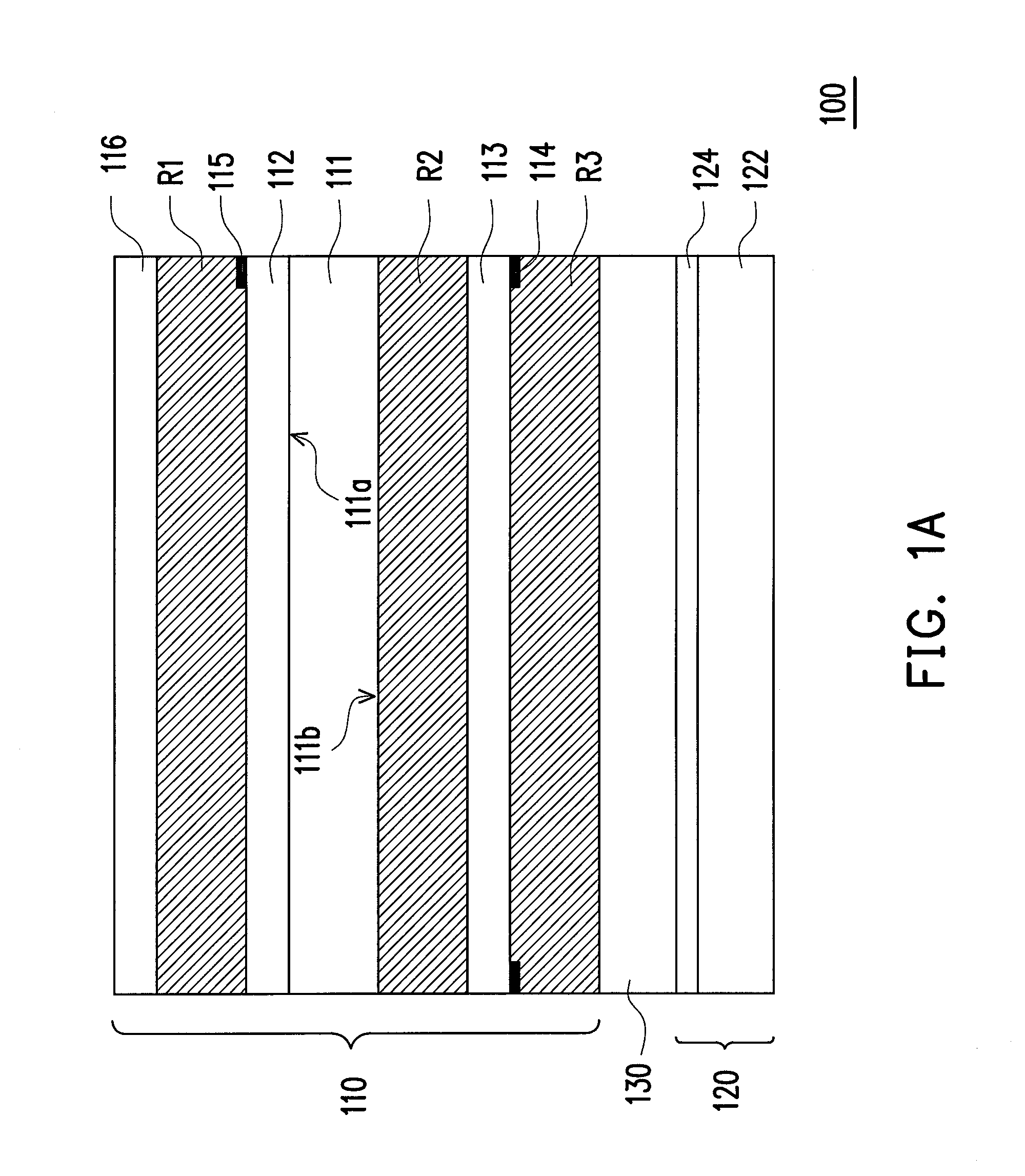
[0027]FIG. 1A illustrates a schematic view of a touch-sensing display apparatus according to one embodiment of the present application. Referring to FIG. 1A, a touch-sensing display apparatus 100 of the present application includes a surface capacitive touch panel 110, an environmentally sensitive electronic device 120, and an adhesive layer 130. Particularly, an overall water / oxygen vapor transmission rate (WVTR / OTR) of the surface capacitive touch panel 110 is lower than 10−1 g / m2*day. Moreover, in some embodiments, the overall WVTR / OTR of the surface capacitive touch panel 110 is lower than 10−2 g / m2*day preferably. In a preferred embodiment the overall WVTR / OTR of the surface capacitive touch panel 110 is lower than 10−3 g / m2*day, for example, the overall WVTR / OTR of the surface capacitive touch panel 110 may be lower than 10−4 g / m2*day, lower than 10−5 g / m2*day or lower than 10−6 g / m2*day.
[0028]The surface capacitive touch panel 110 includes a first substrate 111, a touch-sensi...
PUM
 Abstract
Description
Claims
Application Information


