Semiconductor device

a semiconductor device and semiconductor technology, applied in the field of semiconductor devices, can solve the problems of image pickup defects, image pickup defects, and inability to accurately detect incident light, so as to prevent image pickup defects due to a usage environment and achieve high-quality image data

Active Publication Date: 2011-09-15
SEMICON ENERGY LAB CO LTD
View PDF22 Cites 21 Cited by
  • Summary
  • Abstract
  • Description
  • Claims
  • Application Information

AI Technical Summary

Benefits of technology

[0018]Image pickup defects due to a usage environment can be prevented. Specifically, the semiconductor device can be hardly affected by the intensity of incident light (outside light), and highly accurate image data can be obtained regardless of the intensity of the incident light.

Problems solved by technology

A semiconductor device in which an image is taken using a photo sensor has a problem in that incident light affects the accuracy of image pickup in the semiconductor device when the intensity of the incident light is too high or too low depending on a usage environment or the like.
When the accuracy of image pickup is decreased, image pickup defects such as false recognition of a detection position and blur of a captured image (image data) easily occur.
In particular, the semiconductor device is likely to have the problems when it is affected by light from the outside (outside light).

Method used


Image

  • Semiconductor device
  • Semiconductor device
  • Semiconductor device

Examples


embodiment 1

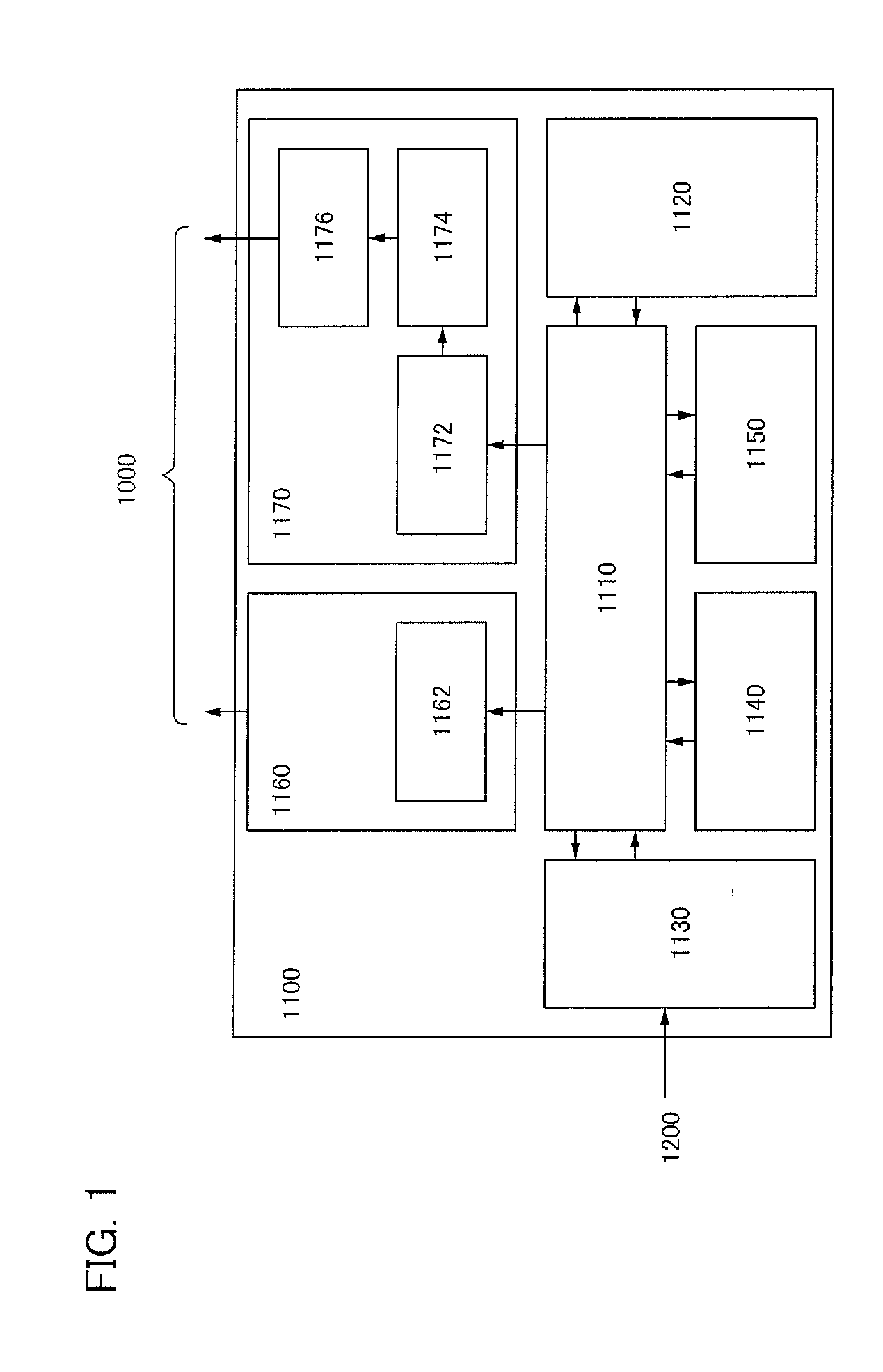
[0038]A semiconductor device in this embodiment has an image pickup function. The semiconductor device includes at least a photo sensor provided in a pixel, a photo sensor provided around the pixel, and a controller. The controller sets the drive condition of the photo sensor provided in the pixel in accordance with the intensity of outside light obtained by the photo sensor provided around the pixel. In the semiconductor device in this embodiment, an image can be taken after the sensitivity of the photo sensor provided in the pixel is changed in accordance with the drive condition set by the controller.

[0039]Note that in the following description, the photo sensor provided in the pixel and the photo sensor provided around (outside) the pixel are also referred to as a first photo sensor and a second photo sensor, respectively.

[0040]A second photo sensor obtains the intensity of light (outside light) which enters the second photo sensor. The controller changes the drive condition of ...

embodiment 2

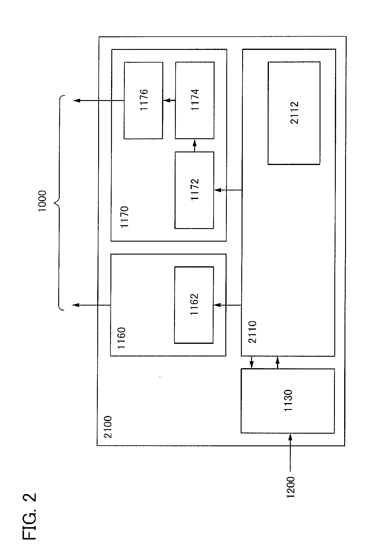
[0068]In this embodiment, a structure of a controller that is different from the structure in Embodiment 1 is described. Note that components which are the same as those in FIG. 1 are denoted by the same reference numerals, and detailed description of such components is omitted.

[0069]In this embodiment, the structure of a controller 2100 illustrated in FIG. 2 can be used. In FIG. 2, the controller 2100 includes an exclusive processing circuit 2110, the register 1130 for outside light intensity data, the timing controller 1160, and the power supply circuit 1170. The exclusive processing circuit 2110 includes a translation table 2112. The timing controller 1160 includes the control data register 1162. The power supply circuit 1170 includes the control data register 1172, the D / A converter 1174, and the amplifier 1176.

[0070]The structure illustrated in FIG. 2 differs from the structure illustrated in FIG. 1 in that the exclusive processing circuit 2110 including the translation table 2...

embodiment 3

[0078]In this embodiment, a semiconductor device which includes the controller described in Embodiment 1 or 2 is described. Here, as semiconductor devices, examples of solid-state image sensors (also referred to as image sensors) are described with reference to FIG. 3, FIG. 4, FIG. 5, FIG. 6, and FIG. 7.

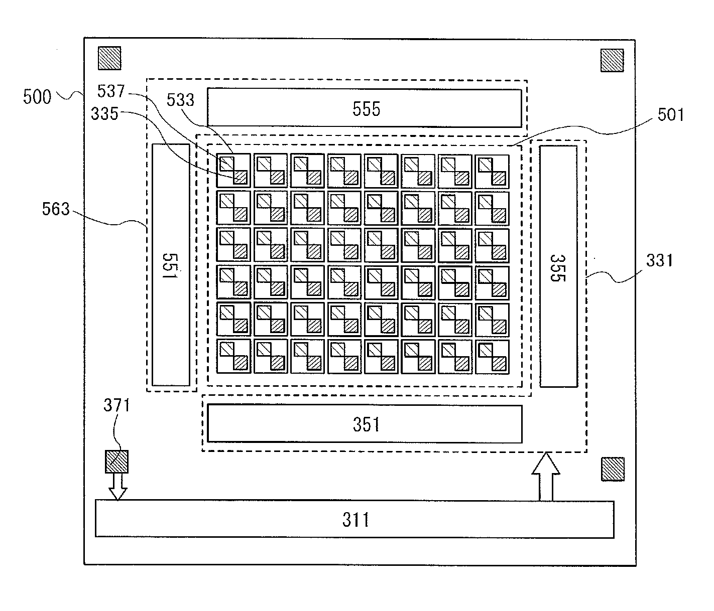
[0079]The structure of a solid-state image sensor is described with reference to FIG. 3. A solid-state image sensor 300 includes a pixel portion 301, a control circuit portion 331, a controller 311, and a sensor portion 371.

[0080]The structure of the controller 1100 illustrated in FIG. 1 in Embodiment 1 or the structure of the controller 2100 described in Embodiment 2 is employed as the structure of the controller 311. The pixel portion 301 includes at least the first photo sensor 1000 described in Embodiment 1 or 2. The sensor portion 371 includes at least the second photo sensor 1200 described in Embodiment 1 or 2.

[0081]The pixel portion 301 includes a plurality of pixels 333 arran...


PUM


Abstract

A semiconductor device obtains highly accurate image data regardless of the intensity of incident light. The semiconductor device includes a first photo sensor provided in a pixel, a second photo sensor provided around the pixel, and a controller for setting the drive condition of the first photo sensor in accordance with the intensity of outside light obtained by the second photo sensor. An image is taken after the sensitivity of the first photo sensor is changed in accordance with the drive condition set by the controller. Thus, in the semiconductor device, an image can be taken using the first photo sensor whose sensitivity is optimized in accordance with the intensity of incident light.

Description

TECHNICAL FIELD[0001]The present invention relates to semiconductor devices and a method for driving the semiconductor devices. In particular, the present invention relates to semiconductor devices including photo sensors and a driving method thereof.BACKGROUND ART[0002]Solid-state image sensors, for example, image sensors have been used for taking images. Further, in recent years, touch panels with input functions obtained by making display devices have image pickup functions have attracted attention. Touch panels are display devices which can be operated when fingers or the like directly touch panels. The touch panels are also referred to as touch screens, for example.[0003]In order to make display devices have image pickup functions, photo sensors are provided in display regions. Thus, the display regions can also serve as input regions. For example, Reference 1 discloses a semiconductor device with an image capture function.REFERENCE[0004][Reference 1] Japanese Published Patent ...

Claims


Application Information

Patent Timeline
Patent Type & Authority Applications(United States)
IPC IPC(8): H04N5/335H01J40/14
CPCG06F3/0412G06F3/0416G06F3/042H01L27/1461H04N5/374H01L27/14645H01L27/14692H04N5/2353H04N5/351H01L27/14612G06F3/04166H04N23/73H04N25/50H04N25/76G06F1/1643
Inventor KUROKAWA, YOSHIYUKIIKEDA, TAKAYUKITAMURA, HIKARU
Owner SEMICON ENERGY LAB CO LTD
Why Eureka
Try Eureka