Electrophoretic display device and electronic apparatus
a display device and display face technology, applied in the field of electrotrophoretic display devices and electronic devices, can solve the problems of variation, deterioration of display devices, and adverse effects on the appearance of display faces, and achieve excellent display characteristics and design properties
- Summary
- Abstract
- Description
- Claims
- Application Information
AI Technical Summary
Benefits of technology
Problems solved by technology
Method used
Image
Examples
first embodiment
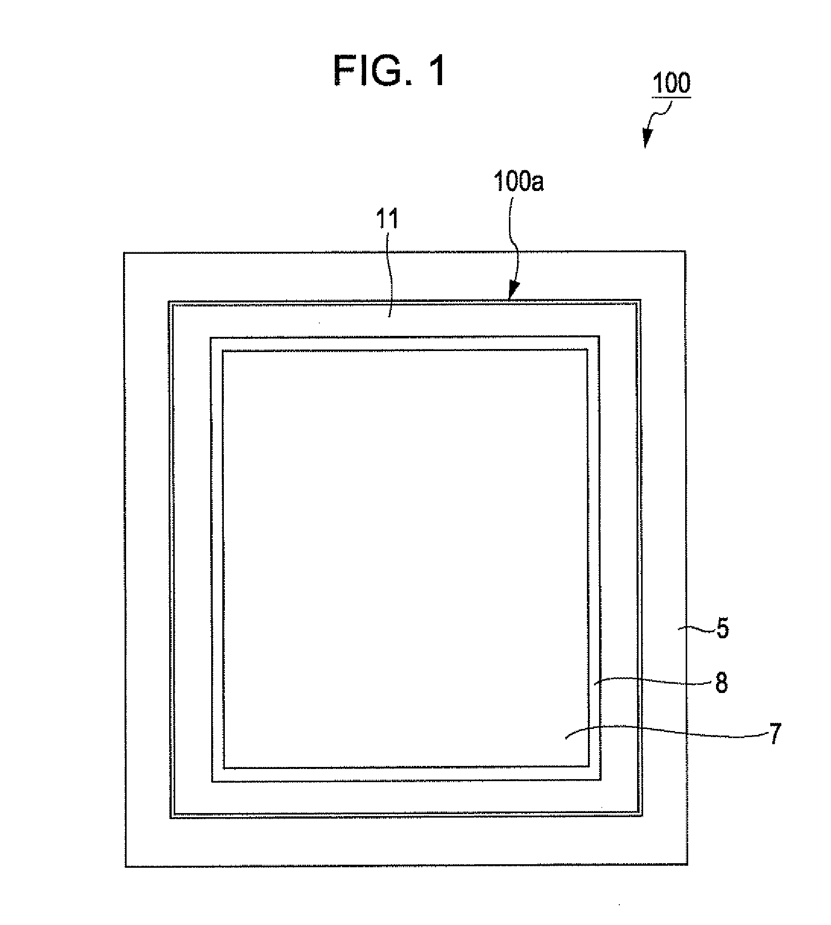
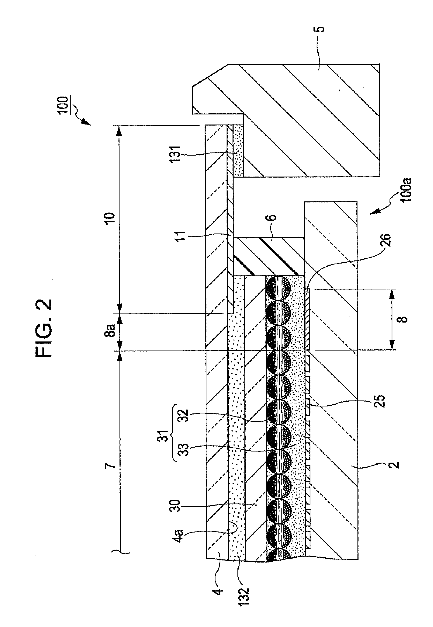
[0031]FIG. 1 is a plan view showing a configuration related to one embodiment of an electrophoretic display device and FIG. 2 is a diagram showing a cross-sectional configuration related to a main section of the electrophoretic display device.
[0032]As shown in FIG. 1, an electrophoretic display device 100 includes a panel section 100a and a casing section 5 which holds the panel section 100a. The panel section 100a includes an element substrate (a first substrate) 2, a transparent substrate 30, an electrophoretic layer 31 which is sandwiched in between these substrates 2 and 30, a glass substrate (a second substrate) 4, and a sealing member 6, as shown in FIG. 2.
[0033]The glass substrate 4 is bonded to the transparent substrate 30 through an adhesive layer 132. The sealing member 6 is disposed between the glass substrate 4 and the element substrate 2 so as to surround the electrophoretic layer 31. The glass substrate 4 is formed in a state where the planar shape thereof extends furt...
second embodiment
[0055]Next, a configuration related to the second embodiment of the electrophoretic display device will be described. A difference between the configurations related to this embodiment and the first embodiment is to adopt the same pixel structure as the display area 7 for the sacrifice display area. Here, the same pixel structure means that as shown in FIG. 4, a plurality of electrodes for sacrifice display 26 each having approximately the same size as the pixel electrode 25 is disposed approximately in a matrix form at the sacrifice display area 8 and a region where each electrode for sacrifice display 26 is formed becomes a pixel region and has a pixel structure 26a capable of displaying various images for each pixel region. A driving layer (not shown) which includes a switching element is provided at each of the electrodes for sacrifice display 26 and the electrode for sacrifice display 26 can be driven independently of the pixel electrode 25. In addition, in other respects, the ...
PUM
 Abstract
Description
Claims
Application Information


