
Stylo-Epitaxial Piezoelectric and Ferroelectric Devices and Method of Manufacturing

a piezoelectric and piezoelectric technology, applied in the direction of device details, device details, generators/motors, etc., can solve the problem of placing very strict requirements on the single crystal substrate, and achieve the effect of improving piezoelectric properties, high volume fraction, and high degree of crystallite orientation

Inactive Publication Date: 2013-04-18
ARMY US SEC THE
View PDF4 Cites 18 Cited by
  • Summary
  • Abstract
  • Description
  • Claims
  • Application Information

AI Technical Summary

Benefits of technology

This patent describes how the crystal structure of a device's ferroelectric grains is aligned with the contacting electrode grains. This alignment results in better performance of the device, as it allows for better polarization and piezoelectric response. This patent is important for improving the functionality of devices that use ferroelectric materials.

Problems solved by technology

The difficulty with this approach is that it places very strict requirements on the single crystal substrate, and the electrode must provide an epitaxial relationship with both the single crystal substrate and the ferroelectric film.

Method used


Image

  • Stylo-Epitaxial Piezoelectric and Ferroelectric Devices and Method of Manufacturing
  • Stylo-Epitaxial Piezoelectric and Ferroelectric Devices and Method of Manufacturing
  • Stylo-Epitaxial Piezoelectric and Ferroelectric Devices and Method of Manufacturing

Examples


Embodiment Construction

[0089]The present invention now will be described more fully hereinafter with reference to the accompanying drawings, in which embodiments of the invention are shown. However, this invention should not be construed as limited to the embodiments set forth herein. Rather, these embodiments are provided so that this disclosure will be thorough and complete, and will fully convey the scope of the invention to those skilled in the art. In the drawings, the thickness of layers and regions may be exaggerated for clarity. Like numbers refer to like elements throughout. As used herein the term “and / or” includes any and all combinations of one or more of the associated listed items.

[0090]The terminology used herein is for the purpose of describing particular embodiments only and is not intended to limit the full scope of the invention. As used herein, the singular forms “a”, “an” and “the” are intended to include the plural forms as well, unless the context clearly indicates otherwise. It wil...


PUM

PropertyMeasurementUnit
thicknessaaaaaaaaaa
lengthaaaaaaaaaa
lengthaaaaaaaaaa

Abstract

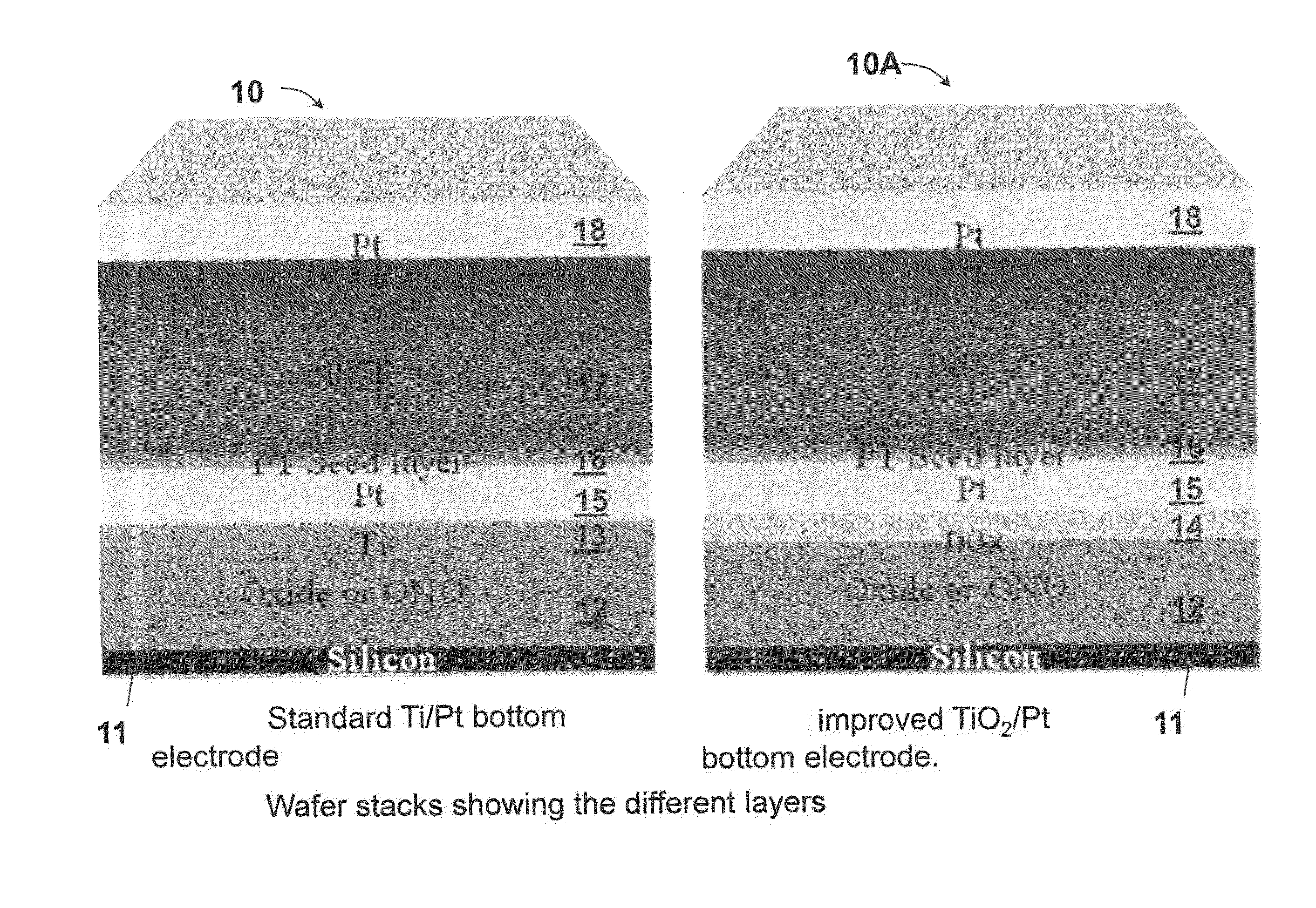
A ferroelectric device comprising a substrate;a textured layer; a first electrode comprising a thin layer of metallic material having a crystal lattice structure divided into granular regions; a seed layer; the seed layer being epitaxially deposited so as to form a column-like structure on top of the granular regions of the first electrode; at least one ferroelectric material layer exhibiting spontaneous polarization epitaxially deposited on the seed layer; the ferroelectric material layer, the seed layer, and first electrode each having granular regions in which column-like structures produce a high degree of polarization normal to the growth plane and a method of making.

Description

CROSS REFERENCE TO RELATED APPLICATIONS[0001]This application claims priority to Provisional Application No. 61 / 547,990 entitled “Stylo Epitaxial Piezoelectric and Ferroelectric Devices and Method of Manufacturing” and Provisional Application No. 61 / 547,879 entitled “Thermally Oxidized Seed Layers for the Production of {001}Textured Electrodes and PZT Capacitors,” by Dr. Glen Fox, et al., both of which were filed on Oct. 17, 2011, and are hereby incorporated by reference.STATEMENT OF GOVERNMENT INTEREST[0002]The embodiments herein may be manufactured, used, and / or licensed by or for the United States Government without the payment of royalties thereon.BACKGROUND OF THE INVENTION[0003]Microelectromechanical systems (MEMS) have been used in a wide range of applications; from pressure sensors and accelerometers to microphones and digital displays. In 2006, STMicroelectronics and Nintendo revolutionized the entire MEMS industry through the launch of the Nintendo Wii gaming console that ...

Claims


Application Information

Patent Timeline
Patent Type & Authority Applications(United States)
IPC IPC(8): H01L41/04C30B19/00H10N30/80
CPCH01L41/081H01L41/0815H01L41/319H01L41/316H01L41/1876H10N30/8554H10N30/079H10N30/078H10N30/706H10N30/708
Inventor FOX, GLEN R.POLCAWICH, RONALD G.POTREPKA, DANIEL M.SANCHEZ, LUZ M.
Owner ARMY US SEC THE
Learn More