This helps you quickly interpret patents by identifying the three key elements:
Problems solved by technology
Method used
Benefits of technology
Benefits of technology
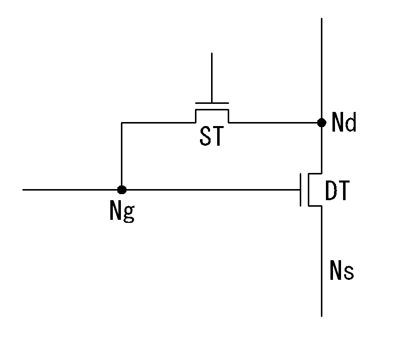
[0012]An organic light emitting diode display device according to the present invention comprises: a display panel having a data line, a scan line, and an emission line formed thereon and a plurality of pixels arranged in a matrix form, each of the pixels comprising: a driving TFT comprising a gate electrode coupled to a first node, a source electrode coupled to a second node, and a drain electrode coupled to a high-potential voltage source supplying a high-potential voltage; an organic light emitting diode comprising an anode coupled to the second node and a cathode coupled
Problems solved by technology
Accordingly, there arises the problem that the luminance of light emitted from the organic light emitti
Method used
Image
Click on the blue label to locate the original text in one second.
Reading with bidirectional positioning of images and text.
Examples
first embodiment
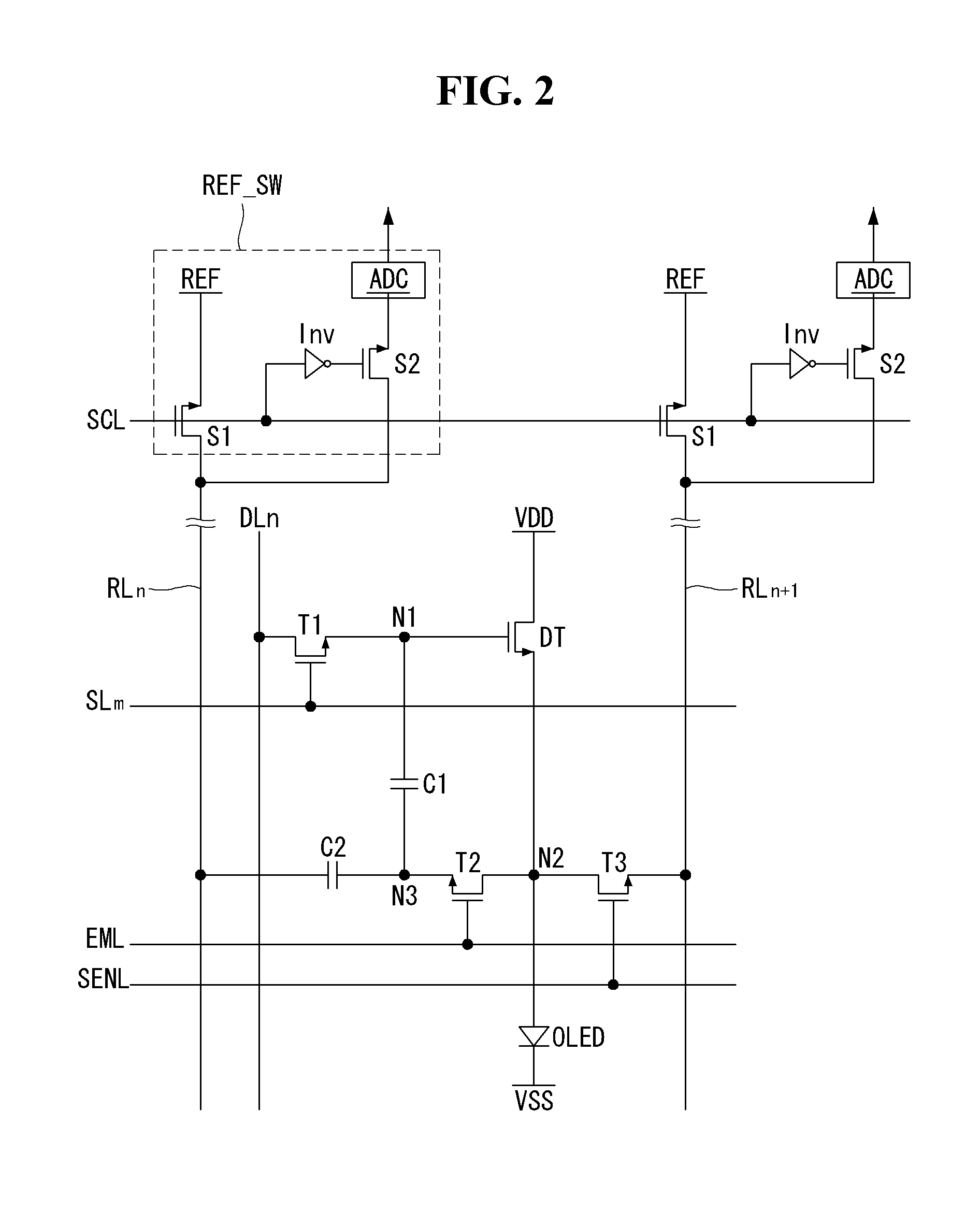
[0044]FIG. 3 is a waveform diagram showing signals which are input into a pixel to make internal compensation according to the present invention. FIG. 3 depicts a data voltage DATA, a high-potential voltage VDD, scan signals SCANm and SCANm+1, an emission signal EM, a sensing signal SEN, and a switching control signal SC which are input into the display panel 10 during one frame period for internal compensation.
[0045]Referring to FIG. 3, the scan signals SCANm, and SCANm+1, the emission signal EM, and the sensing signal SEN are signals for controlling the first to third TFTs T1, T2, and T3 of the pixel P. The switching control signal is a signal for controlling the first and second switches S1 and S2 of the reference voltage switching circuit REF SW.
[0046]The high-potential voltage VDD, the scan signals SCANm and SCANm+1, the emission signal EM, the sensing signal SEN, and the switching control signal SC are generated every frame period. One frame period comprises a first vertical b...
second embodiment
[0088]FIG. 8 is a waveform diagram showing signals which are input into a pixel to make internal compensation according to the present invention. FIG. 8 depicts a data voltage DATA, a high-potential voltage VDD, scan signals SCANm and SCaNm+1, an emission signal EM, a sensing signal SEN, and a switching control signal SC which are input into the display panel 10 during one frame period to make internal compensation.
[0089]The signals input into the pixel P according to the second embodiment of the present invention are similar to the signals input into the pixel P according to the first embodiment of the present invention described in conjunction with FIG. 3, except for the high-potential voltage VDD and the sensing signal SEN. Accordingly, descriptions of the data voltage DATA, scan signals SCANm and SCaNm+1, emission signal EM, and switching control signal SC, among the signals input into the pixel P according to the second embodiment of the present invention, will be omitted.
[0090...
PUM
Abstract
An organic light emitting diode display device comprises: a display panel having a plurality of pixels, each of the pixels comprising: a driving TFT comprising a gate electrode coupled to a first node, a source electrode coupled to a second node, and a drain electrode coupled to a high-potential voltage source; an organic light emitting diode comprising an anode coupled to the second node and a cathode coupled to a low-potential voltage source; a first TFT in response to a scan signal having a first logic level voltage to connect the first node to a data line; a second TFT in response to an emission signal having the first logic level voltage to connect the second node to the third node; a first capacitor coupled between the first node and the third node; and a second capacitor coupled between the third node and a reference voltage source.
Description
[0001]This application claims the benefit of Korean Patent Application No. 10-2011-0121137 filed on Nov. 18, 2011, which is incorporated by reference herein in its entirety.BACKGROUND[0002]1. Technical Field[0003]This document relates to an organic light emitting diode display device capable of compensating the threshold voltage of a driving TFT.[0004]2. Description of the Related Art[0005]The demand for various types of display devices for displaying an image is increasing. Various flat panel displays, such as a liquid crystal display, a plasma display panel, and an organic light emitting diode (OLED) display, have been recently used. Out of the various types of flat panel displays, the OLED display has excellent characteristics including a low voltage drive, a thin profile, a wide viewing angle, and a fast response time. Especially, an active matrix type OLED display for displaying an image on a plurality of pixels, which are arranged in a matrix form, has been widely used.[0006]A...
Claims
Application Information
Patent Timeline
Application Date:The date an application was filed.
Publication Date:The date a patent or application was officially published.
First Publication Date:The earliest publication date of a patent with the same application number.
Issue Date:Publication date of the patent grant document.
PCT Entry Date:The Entry date of PCT National Phase.
Estimated Expiry Date:The statutory expiry date of a patent right according to the Patent Law, and it is the longest term of protection that the patent right can achieve without the termination of the patent right due to other reasons(Term extension factor has been taken into account ).
Invalid Date:Actual expiry date is based on effective date or publication date of legal transaction data of invalid patent.
