Method and apparatus for testing light-emitting device

a technology of light-emitting devices and methods, which is applied in the direction of optical radiation measurement, instruments, television systems, etc., can solve the problems of shade, inability to detect conventional electrical tests, and failures caused by manufacturing process or material defects

Active Publication Date: 2013-08-08
EPISTAR CORP
View PDF20 Cites 31 Cited by
  • Summary
  • Abstract
  • Description
  • Claims
  • Application Information

AI Technical Summary

Problems solved by technology

However, some types of failures caused by the manufacturing process or material defects, such as the current leakage in a small local area or a surface stain / damage which causes the light shaded, cannot be detected by a conventional electrical test.
For a light-emitting device comprises a plurality of light-emitting diodes connected in series and / or parallel, if only a few light-emitting diodes fail, it is difficult to be detected by a conventional electrical test.
Besides, the uniformity of the luminous intensity of the plurality of light-emitting diodes which often concerns the application cannot be measured in the conventional electrical test as well.

Method used


Image

  • Method and apparatus for testing light-emitting device
  • Method and apparatus for testing light-emitting device
  • Method and apparatus for testing light-emitting device

Examples


Embodiment Construction

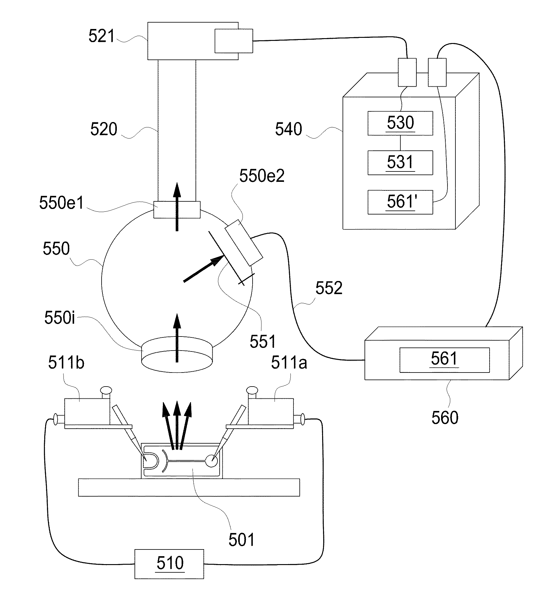
[0011]The light-emitting device to be tested in the present application comprises a plurality of light-emitting diodes. The plurality of light-emitting diodes may be formed in a series connection, a parallel connection, or both series and parallel connection. The light-emitting device may be in a variety of forms. For example, the light-emitting device to be tested may be at a chip level (or wafer level) or a package level. For the light-emitting device at a chip level, the light-emitting device can be a chip having one light-emitting diode, or a chip comprises multiple light-emitting diodes monolithically integrated together. For the light-emitting device at a wafer level, the light-emitting device is in a wafer form with a plurality of light-emitting diodes, wherein the wafer can be separated later to form multiple chips which each contains one or more light-emitting diodes by dicing. For the light-emitting device at a package level, the light-emitting device can be one package co...


PUM


Abstract

Disclosed is a method for testing a light-emitting device comprising the steps of: providing an integrating sphere comprising an inlet port and a first exit port; disposing the light-emitting device close to the inlet port of the integrating sphere; providing a current source to drive the light-emitting device to form an image of the light-emitting device in driven state; providing an image receiving device and to receive the image of the light-emitting device, wherein the image receiving device is connected to the first exit port of the integrating sphere; and determining a luminous intensity of the light-emitting device according to the image. An apparatus for testing a light-emitting device is also disclosed. The apparatus for testing a light-emitting device comprises: an integrating sphere comprising an inlet port and a first exit port, wherein the light-emitting device is disposed close to the inlet port of the integrating sphere; an image receiving device connected to the first exit port of the integrating sphere for receiving an image of the light-emitting device; and a processing unit coupled to image receiving device for determining a luminous intensity of the light-emitting device.

Description

CROSS REFERENCE TO RELATED APPLICATION[0001]This application is a continuation-in-part of U.S. patent application, Ser. No. 13 / 365,820, entitled “METHOD AND APPARATUS FOR TESTING LIGHT-EMITTING DEVICE”, filed on Feb. 3, 2012, now pending, which disclosure is incorporated herein by reference in its entirety and made a part of this specification.TECHNICAL FIELD[0002]The application relates to a method and apparatus for testing a light-emitting device.DESCRIPTION OF BACKGROUND ART[0003]As the technology of the light-emitting diodes (LEDs) develops, the light-emitting diodes are applied widely. And now a light-emitting device adopting the light-emitting diode usually comprises more than one single light-emitting diode. For example, the light-emitting device such as a High Voltage Light-Emitting Diode (HVLED), an Alternating Current Light-Emitting Diode (ACLED), or an Array that is commonly used as a display, a traffic sign, and a lighting, etc., comprises a plurality of light-emitting d...

Claims


Application Information

Patent Timeline
Patent Type & Authority Applications(United States)
IPC IPC(8): G01J1/04
CPCG01J1/0474G01J2001/4252G01R31/2635G01J1/4228G01J2001/0481
Inventor CHAO, TANG-CHUNGTSENG, PEI-HSIANGKUO, JIA-KUANWU, GUAN-HUNGSU, YUAN-HAOHO, CHI-HSINHSU, CHIA-LIANGLU, CHIH-CHIANG
Owner EPISTAR CORP
Why Eureka
Try Eureka