
Wiring substrate

a technology of wiring substrate and wiring plate, which is applied in the direction of final product manufacturing, printed circuit aspects, stacked spaced pcbs, etc., can solve the problems of increasing the number of parts, increasing and increasing so as to prevent the miniaturization of the wiring substrate, the cost of manufacturing a wiring substrate increases, and the time for assembling is longer

Inactive Publication Date: 2014-01-30
TOYOTA IND CORP
View PDF8 Cites 5 Cited by
  • Summary
  • Abstract
  • Description
  • Claims
  • Application Information

AI Technical Summary

Benefits of technology

The patent text aims to provide a wiring substrate that can be connected with another member without adding extra parts, and can be positioned with respect to the other member without orientation restrictions. This would allow for the miniaturization of the wiring substrate and the prevention of space requirement for additional members.

Problems solved by technology

When such additional members are used, for example, the number of parts increases, longer time for assembling is required, and costs for manufacturing a wiring substrate increase.
In addition, space for the additional members is required in the substrate.
Thus, it is impossible to position the two substrates in a manner that the surfaces of the two substrates are arranged in parallel.

Method used


Image

  • Wiring substrate
  • Wiring substrate
  • Wiring substrate

Examples


first embodiment

[0039]A wiring substrate according to a first embodiment of the invention will be described with reference to the drawings.

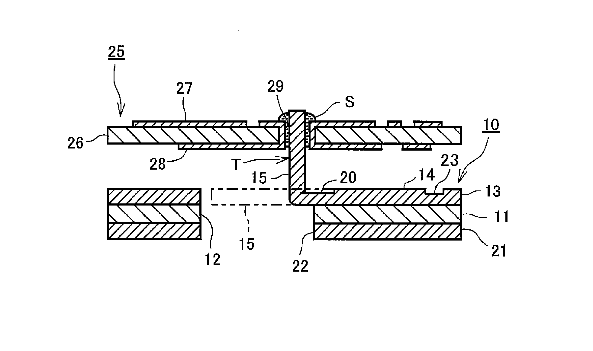
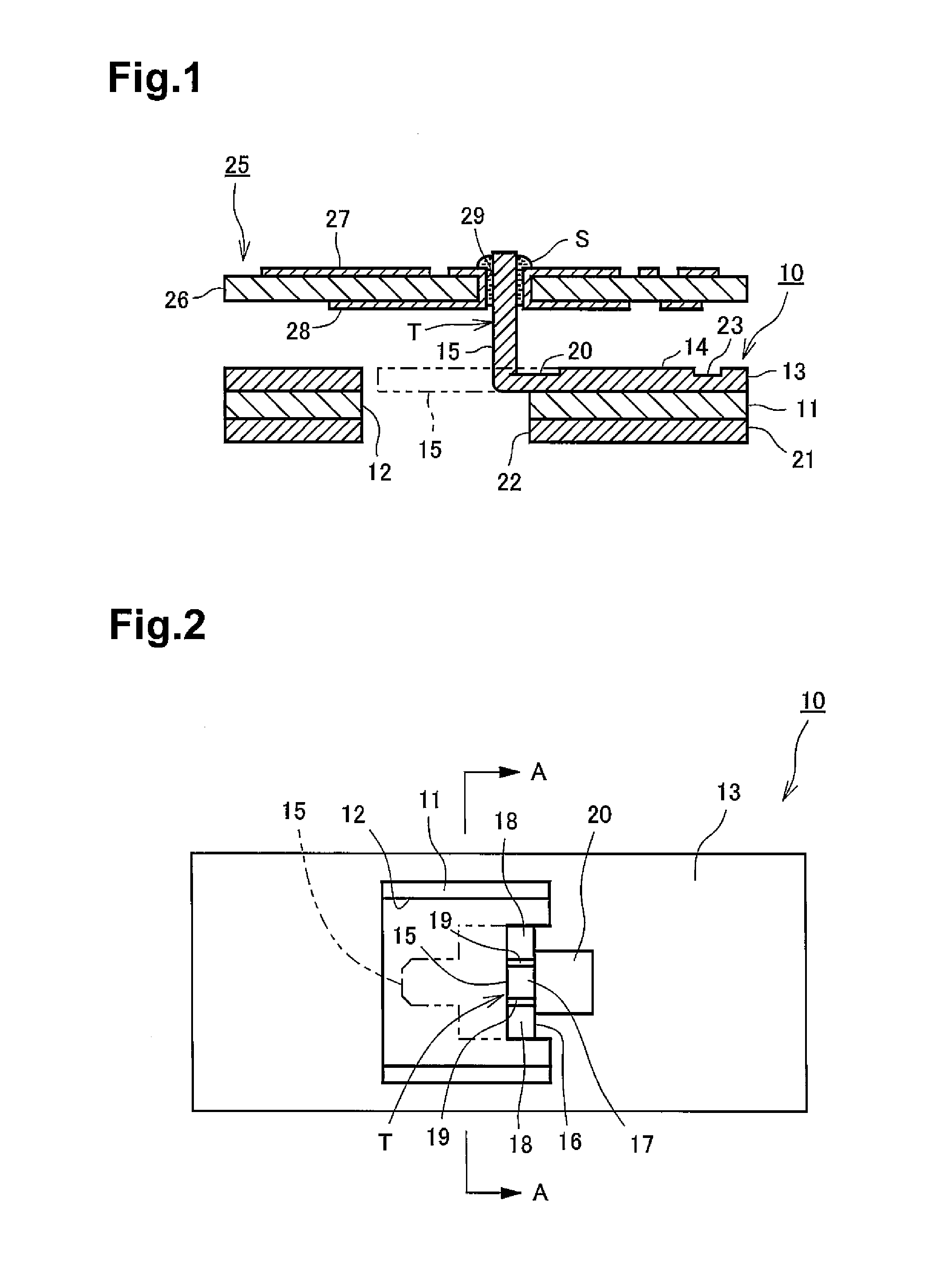
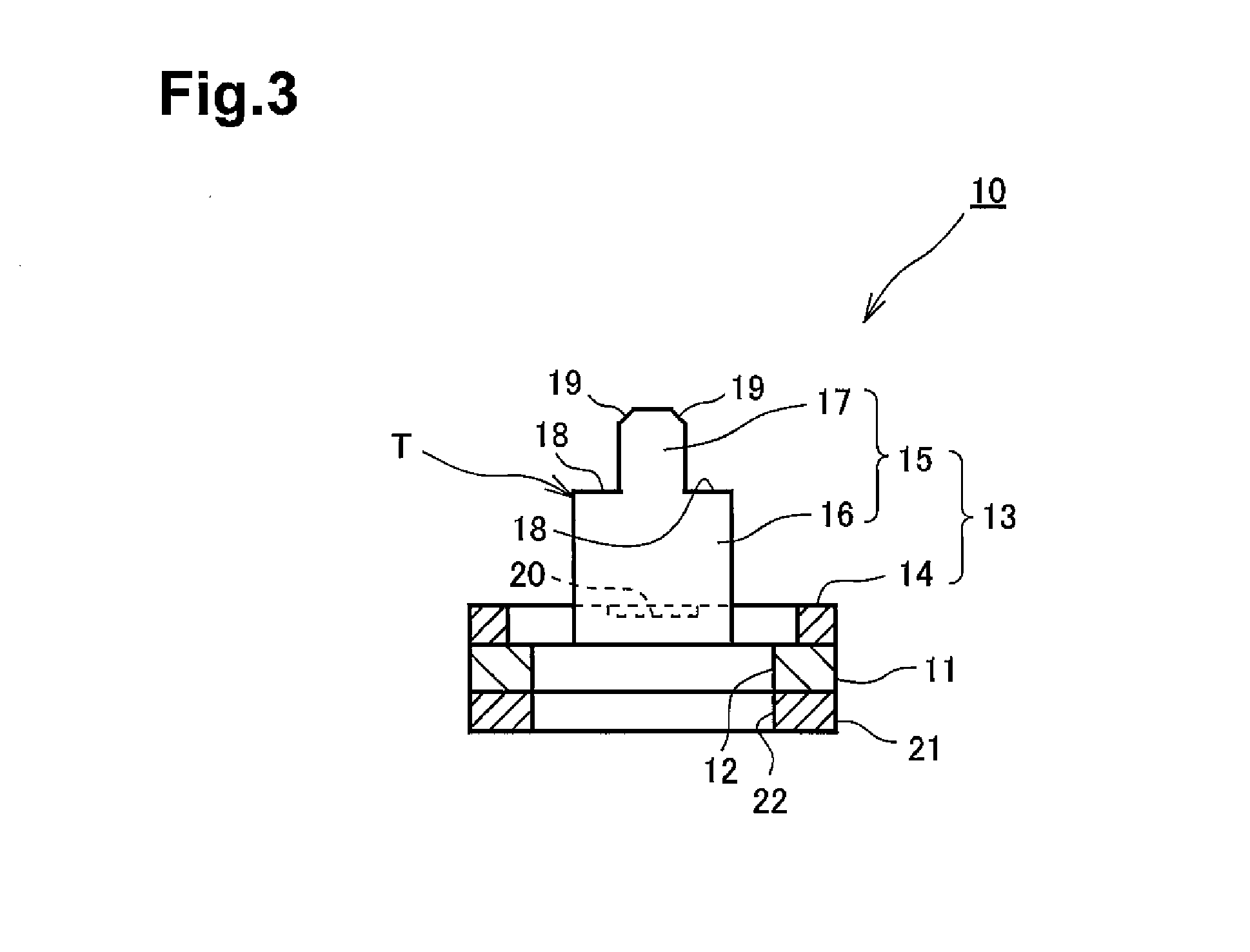
[0040]A wiring substrate 10 of the first embodiment as illustrated in FIG. 1 is a power board controlled by, for example, a control board of a high-output motor of an electric vehicle or a hybrid vehicle. The wiring substrate 10 is fixed to a non-illustrated housing via a heat dissipation sheet. In the wiring substrate 10, as illustrated in FIG. 1, a front wiring pattern 13 in the form of plate is fixed to the front surface of the insulating layer 11 via a non-illustrated adhesive sheet and a back wiring pattern 21 is fixed to the back surface of the insulating layer 11 via a non-illustrated adhesive sheet. That is, the wiring substrate 10 are integrally formed from the insulating layer 11, the front wiring pattern 13 and the back wiring pattern 21. The wiring substrate 10 of FIG. 1 is connected with a substrate 25, which is another member, via a connection term...

second embodiment

[0067]Next, a wiring substrate according to the second embodiment will be described. In the wiring substrate of the second embodiment, a back wiring pattern includes an extended portion and the connection terminal is formed by bending the extended portion. Like elements as in the first embodiment are denoted as like numerals and explanation of such like elements are omitted.

[0068]As illustrated in FIG. 6A, a front wiring pattern 41 of this embodiment is fixed to the upper surface of the insulating layer 11. The front wiring pattern 41 overlaps with the insulating layer 11 and includes an opening 42 that has the substantially the same shape as the opening 12 of the insulating layer 11. The front wiring pattern 41 and the back wiring pattern 43 may be electrically connected between the layers.

[0069]The back wiring pattern 43 includes a joint portion 44 that overlaps with the insulating layer 11 and an extended portion 45 that extends from the joint portion 44 toward the opening 12. Th...

third embodiment

[0076]Next, a wiring substrate according to the third embodiment will be described. In the wiring substrate of the third embodiment, an internal wiring pattern provided between a plurality of insulating layers includes an extended portion. Like elements as in the first and second embodiments are denoted as like numerals and explanation of such like elements are omitted.

[0077]As illustrated in FIG. 7A, a wiring substrate 60 of this embodiment includes a front wiring pattern 41, a back wiring pattern 21, an internal wiring pattern 65, a first insulating layer 61 and a second insulating layer 63. The front wiring pattern 41 overlaps with the first insulating layer 61 and includes an opening 42 that is substantially the same as an opening 62 of the first insulating layer 61. The back wiring pattern 21 overlaps with the second insulating layer 63 and includes an opening 22 that is substantially the same as an opening 64 of the second insulating layer 63.

[0078]The internal wiring pattern ...


PUM


Abstract

A wiring substrate (10, 40, 60, 80) includes a wiring pattern (13, 21, 41, 43, 65, 83a, 83b, 83c) and an insulating layer (11, 26, 48, 81) to which the wiring pattern is fixed. The insulating layer includes an edge. The wiring pattern (13, 21, 41, 43, 65, 83a, 83b, 83c) includes a joint portion (14, 44, 66) connected with the insulating layer (11, 26, 48, 81) and an extended portion (45, 45, 67, 85) that extends from the joint portion (14, 44, 66) and protrudes from the edge of the insulating layer (11, 26, 48, 81). The insulating layer (11, 26, 48, 81) or the joint portion (14, 44, 66) includes an outermost surface. A connection terminal (T, T1) is provided by bending the extended portion (45, 45, 67, 85) so that a part of the extended portion (45, 45, 67, 85) is protruded from the outermost surface of the insulating layer (11, 26, 48, 81) or the joint portion (14, 44, 66).

Description

TECHNICAL FIELD[0001]The present invention relates to a wiring substrate that is preferably used for an electronic device in an electric vehicle or a hybrid vehicle.BACKGROUND ART[0002]Conventionally, as a technique pertaining to a wiring substrate, for example, there is a power supply as disclosed in Patent Document 1. In this power supply, a power board and a control board are integrally connected to each other and electrically connected via hard wires in the form of metal rods. Alternatively, the power board and the control board are connected by providing a connector in the power board and inserting the control board in the connector.[0003]As another prior art, for example, a connecting structure between the print boards as disclosed in Patent Document 2 is known. In this connecting structure, a first print board includes an insulating plate, pairs of upper and lower lands and through-holes each extends through the corresponding pair of the upper and lower lands. A second print ...

Claims


Application Information

Patent Timeline
IPC IPC(8): H05K1/02
CPCH05K1/02H05K1/144H05K3/368H05K3/4092H05K2201/0397H05K2201/042H05K2201/09063H05K2201/09745H05K2201/1031H05K2203/0195H05K2203/0323Y02P70/50
Inventor SHIMADU, HITOSHISAWADA, TAKEHIKOHAYAKAWA, TAKAHIROASAI, TOMOAKIYAMAUCHI, RYOU
Owner TOYOTA IND CORP
Learn More