Organic light emitting diode display device and method of manufacturing the same

a light-emitting diode and display device technology, applied in the direction of thermoelectric device junction materials, semiconductor devices, electrical devices, etc., to achieve the effect of improving light extraction efficiency

Active Publication Date: 2014-03-06
LG DISPLAY CO LTD
View PDF10 Cites 55 Cited by
  • Summary
  • Abstract
  • Description
  • Claims
  • Application Information

AI Technical Summary

Benefits of technology

[0012]An aspect of the present invention is directed to provide an OLED display device with enhanced light extraction efficiency and a method of manufacturing the same.

Problems solved by technology

OLED display devices are current driving devices, and use a complicated driving circuit compared to LCD devices.
Also, each sub-pixel includes a complicated compensation circuit, for emitting desired color light during a desired time.

Method used


Image

  • Organic light emitting diode display device and method of manufacturing the same
  • Organic light emitting diode display device and method of manufacturing the same
  • Organic light emitting diode display device and method of manufacturing the same

Examples


Embodiment Construction

[0023]Reference will now be made in detail to the exemplary embodiments of the present invention, examples of which are illustrated in the accompanying drawings. Wherever possible, the same reference numbers will be used throughout the drawings to refer to the same or like parts.

[0024]Hereinafter, embodiments of the present invention will be described in detail with reference to the accompanying drawings.

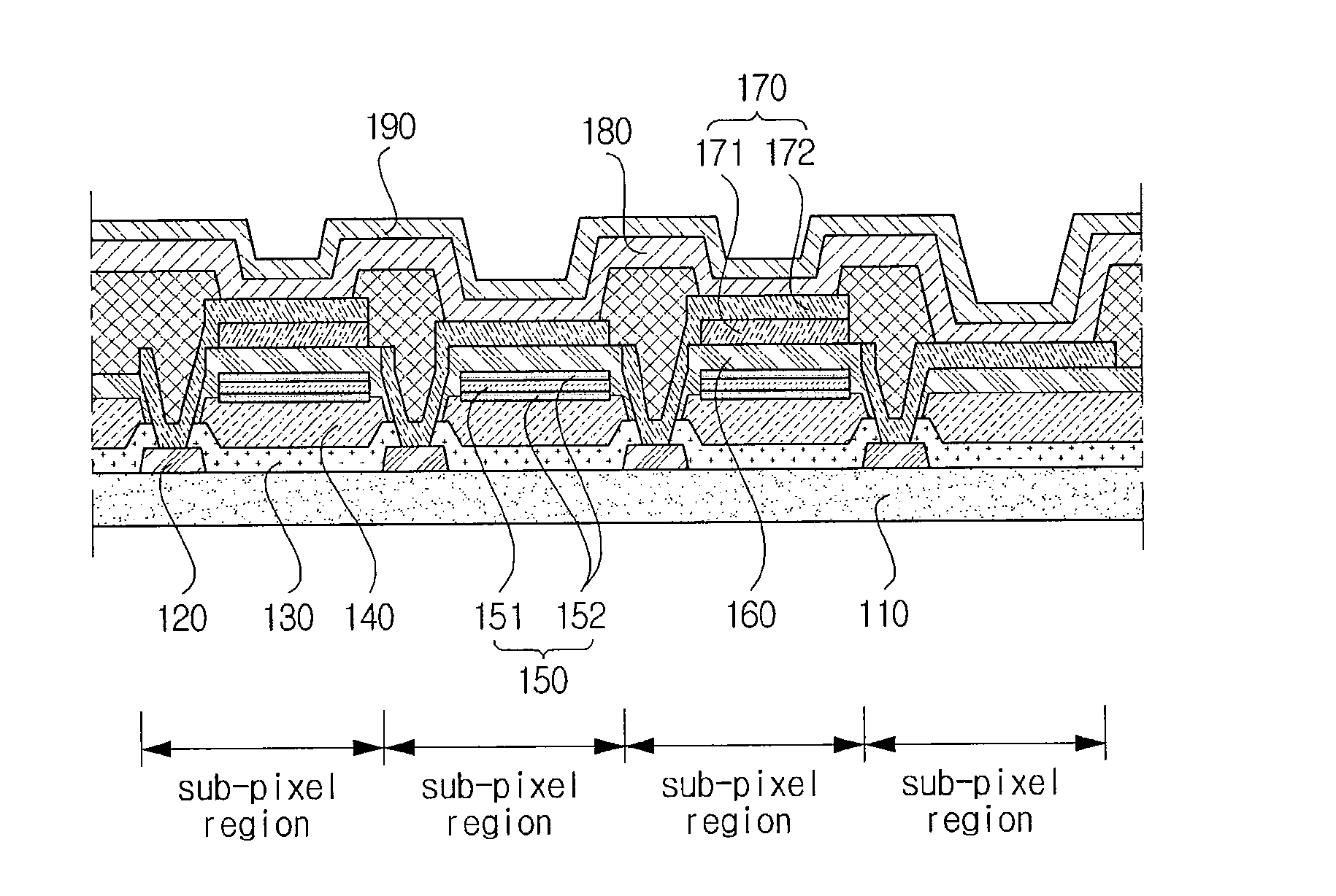
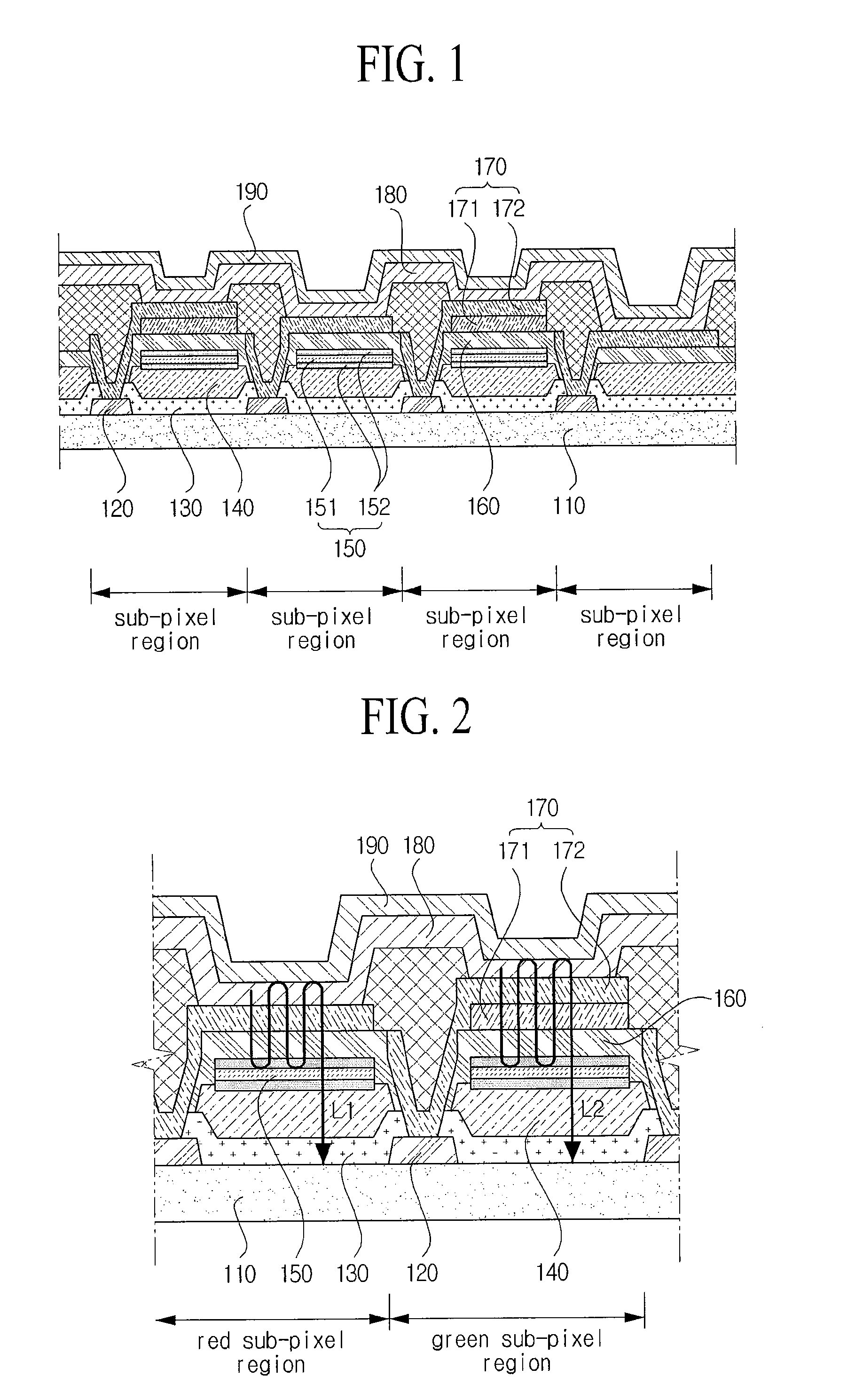
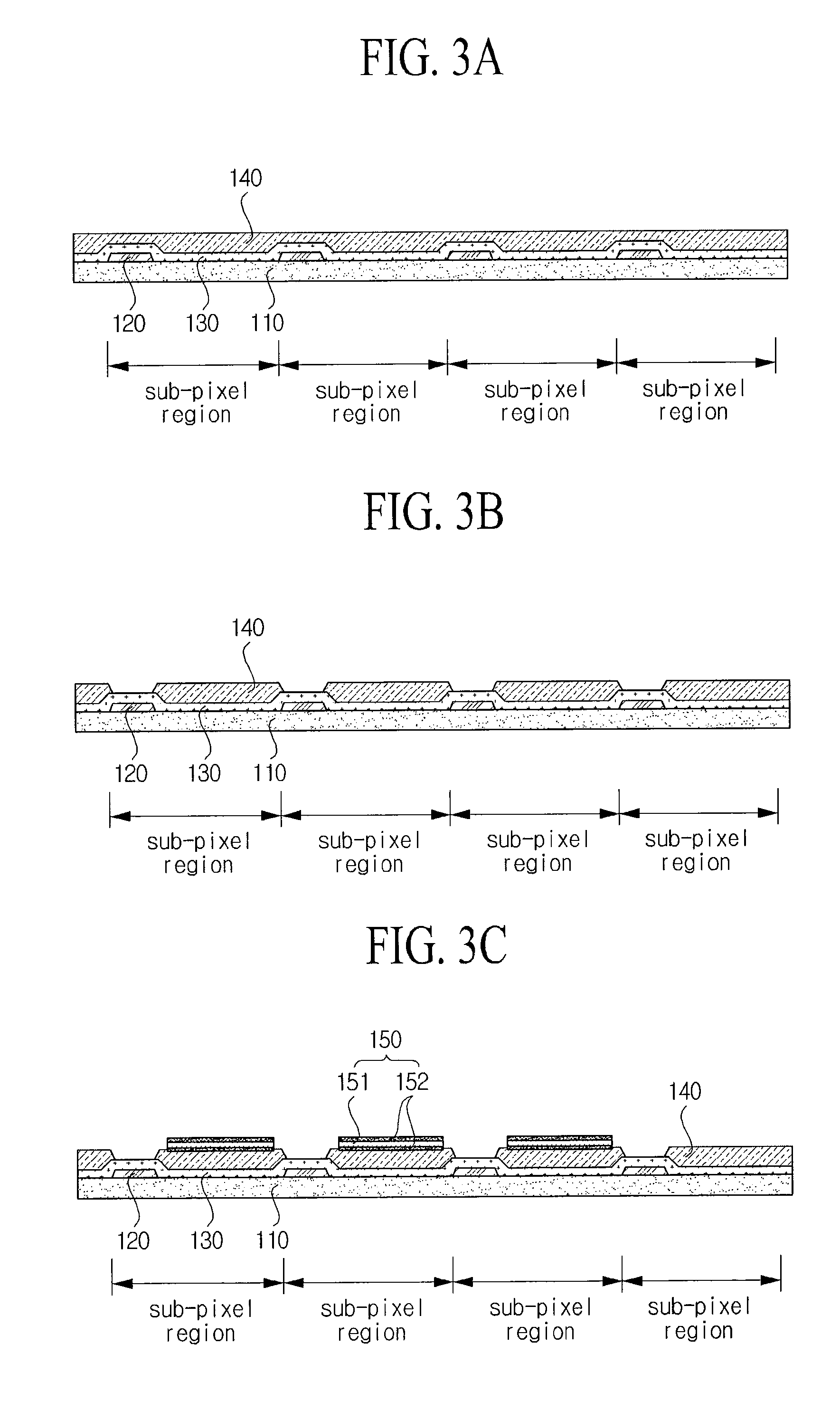
[0025]FIG. 1 is a sectional view illustrating an OLED display device according to an embodiment of the present invention.

[0026]As illustrated in FIG. 1, the OLED display device according to an embodiment of the present invention includes a substrate 110, a thin film transistor 120, an insulating layer 130, a planarizion layer 140, a semitransparent reflective layer 150, a protective layer 160, an anode electrode 170, an organic light emitting layer 180, and a cathode electrode 190.

[0027]The substrate 10 may be formed of glass, a transparent flexible material, or an opaque insulating...


PUM


Abstract

An OLED display device is provided. The OLED display device includes a substrate segmented into a plurality sub-pixel regions, a thin film transistor formed in each of the sub-pixel regions, an insulating layer and a planarizion layer formed on the thin film transistor, a semitransparent reflective layer selectively formed in each sub-pixel region on the planarizion layer, a protective layer formed on the semitransparent reflective layer, an anode electrode formed in a region corresponding to the semitransparent reflective layer on the protective layer and connected to the thin film transistor, an organic light emitting layer connected to the anode electrode, and emitting light, and a cathode electrode formed on the organic light emitting layer.

Description

CROSS-REFERENCE TO RELATED APPLICATIONS[0001]This application claims priority to the Korean Patent Application No. 10-2012-0094094 filed on Aug. 28, 2012, the entirety of which is hereby incorporated by reference herein.BACKGROUND[0002]1. Field of the Invention[0003]The present invention relates to an organic light emitting diode (OLED) display device and a method of manufacturing the same, and more particularly, to an active-matrix OLED (AMOLED) display device and a method of manufacturing the same.[0004]2. Discussion of the Related Art[0005]Recently, as the information age has come and research on flat panel display devices continues to accelerate, OLED display devices posterior to liquid crystal display (LCD) devices are being actively developed as next-generation flat panel display devices.[0006]Since OLED display devices are self-emitting devices, the OLED display devices do not need a backlight unlike LCD devices, and thus can be more lightened and thinned than the LCD devices...

Claims


Application Information

Patent Timeline
Patent Type & Authority Applications(United States)
IPC IPC(8): H01L27/32H01L51/56
CPCH01L51/56H01L27/3244H10K59/30H10K59/351H10K50/852H10K50/856H10K59/35H10K59/122H10K59/12H10K59/125H10K59/126H10K71/00
Inventor KIM, SE JUNELEE, JOON SUKKIM, YONG CHULSHIM, SUNG BIN
Owner LG DISPLAY CO LTD
Why Eureka
Try Eureka