Stretchable electronic device and method of manufacturing same

a technology of electronic devices and strechable parts, applied in the direction of circuit bendability/stretchability, printed circuit non-printed electric components association, semiconductor/solid-state device details, etc., can solve the problem of difficult application to a large area, difficult to apply fine patterning of a micrometer level, and the restriction of strechability of strechable electronic devices. to achieve the effect of reducing or eliminating the open of coil interconnection

Active Publication Date: 2014-04-17
ELECTRONICS & TELECOMM RES INST
View PDF7 Cites 30 Cited by
  • Summary
  • Abstract
  • Description
  • Claims
  • Application Information

AI Technical Summary

Benefits of technology

[0010]The inventive concept also provides a stretchable electronic device and a method of manufacturing the same that may minimize or remove the open of coil interconnection.

Problems solved by technology

However, a typical stretchable electronic device experiences the restriction of the strechability of the metal interconnection by the amount of the pre-strain initially applied to a substrate.
In addition, the wave-shaped metal interconnection has a drawback that it is difficult to be applied to a large area and ensure reliability, because its manufacturing processes are complex compared to general semiconductor device manufacturing processes.
However, the conductive stretchable material may have drawbacks that it has higher electric resistance compared to metal while having high expandability and it has a difficulty in applying fine patterning of a micrometer level.
However, the spring-shaped interconnection has a limit in increasing an expanding rate because strain is locally concentrated on only a specific part of interconnection and damage occurs when being stretched.

Method used


Image

  • Stretchable electronic device and method of manufacturing same
  • Stretchable electronic device and method of manufacturing same
  • Stretchable electronic device and method of manufacturing same

Examples


Embodiment Construction

[0033]It should be construed that foregoing general illustrations and following detailed descriptions are exemplified and an additional explanation of claimed inventions is provided. Therefore, the inventive concept may, however, be embodied in different forms and should not be construed as limited to the embodiments set forth herein. Rather, these embodiments are provided so that this disclosure will be thorough and complete, and will fully convey the scope of the inventive concept to those skilled in the art. If the specification describes that a certain part includes a certain component, this means that it may further include other different components. In addition, an embodiment described and exemplified herein includes a complementary embodiment thereof. Embodiments of the inventive concept will be described in detail below with reference to the accompanying drawings.

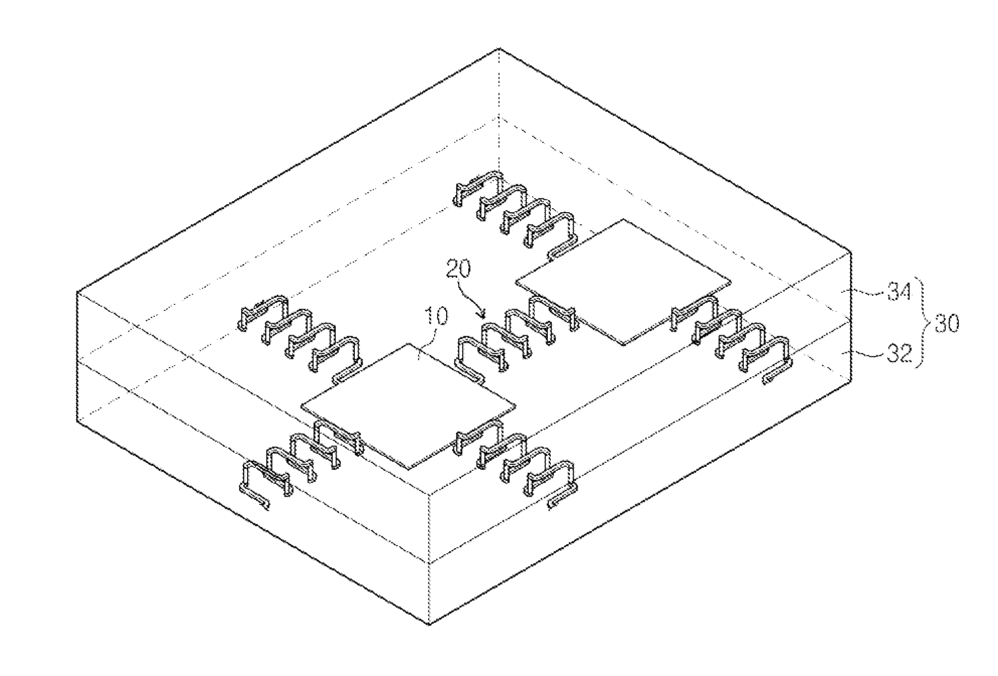
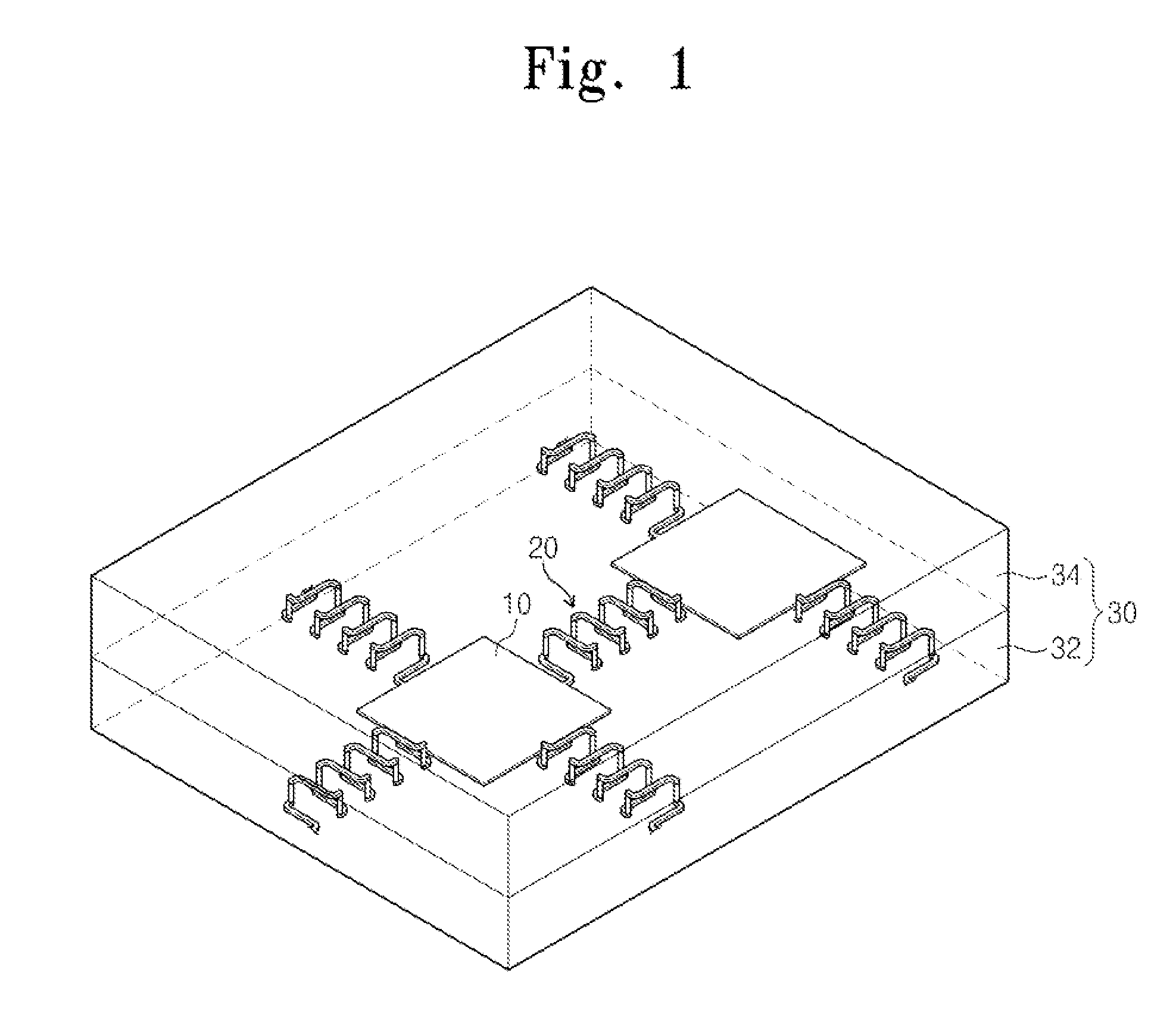
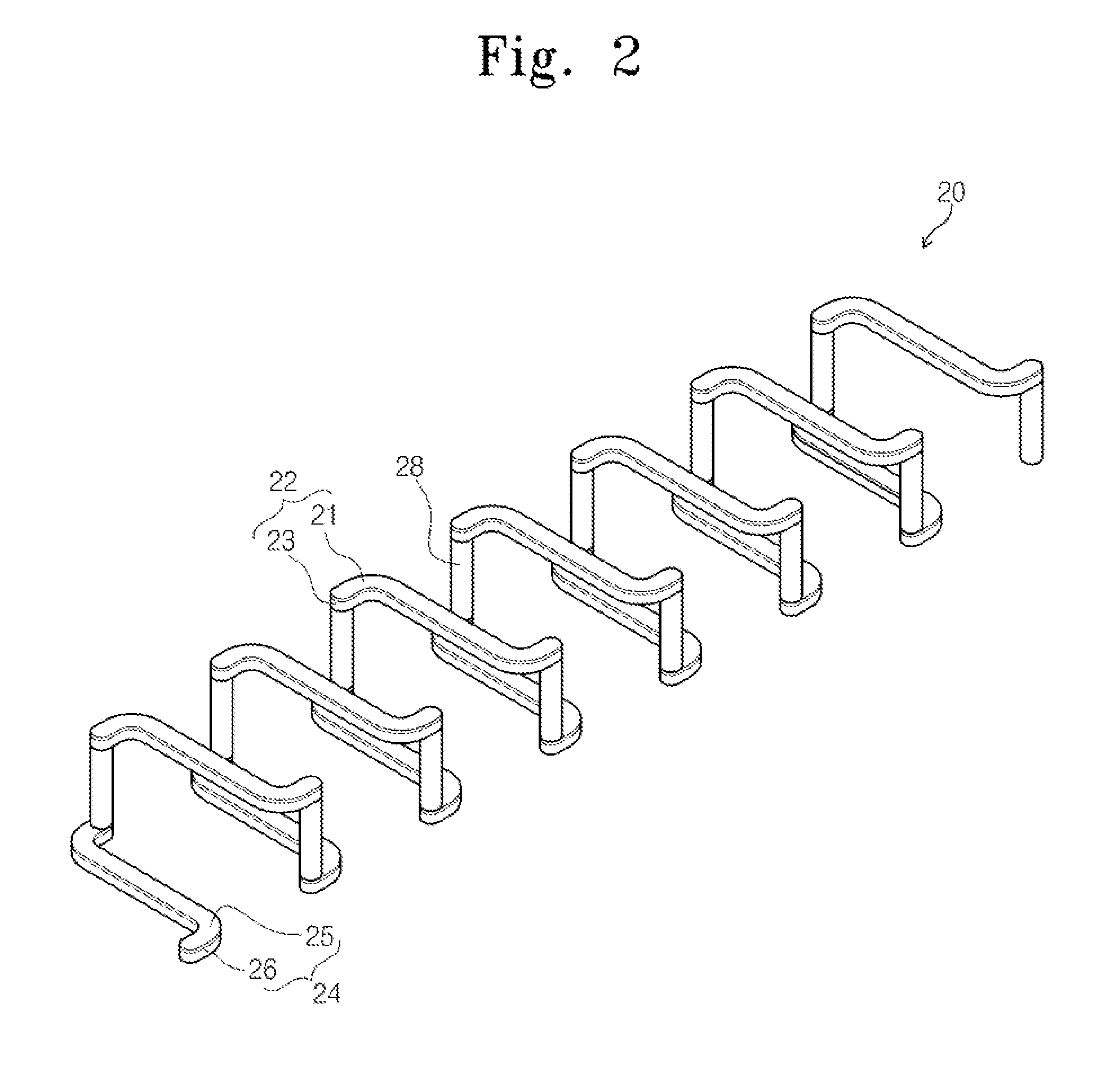
[0034]FIG. 1 is a perspective view schematically representing a stretchable electronic device according to an em...


PUM


Abstract

Provided are a stretchable electronic device and a method of manufacturing the same. The manufacturing method includes forming coil interconnection on a first substrate, forming a first stretchable insulating layer that covers the coil interconnection, forming a second substrate on the first stretchable insulating layer, separating the first substrate from the coiling interconnection and the first stretchable insulating layer, and forming a transistor on the coil interconnection.

Description

CROSS-REFERENCE TO RELATED APPLICATIONS[0001]This U.S. non-provisional patent application claims priority under 35 U.S.C. §119 of Korean Patent Application No. 10-2012-0115432, filed on Oct. 17, 2012, the entire contents of which are hereby incorporated by reference.BACKGROUND OF THE INVENTION[0002]The inventive concept disclosed herein relates to an electronic device and a method of manufacturing the same and more particularly, to a stretchable electronic device and a method of manufacturing the same.[0003]A stretchable electronic device may maintain electrical functions even if a substrate is expanded by the stress applied from the outside. The stretchable electronic device has applicability in various fields, including sensor skin for a robot, a wearable communication element, a bio element embedded in / attached to a human body, a next-generation display beyond the limits of a simple bendable and / or flexible element.[0004]A typical stretchable electronic device has a structure in ...

Claims


Application Information

Patent Timeline
Patent Type & Authority Applications(United States)
IPC IPC(8): H05K1/02H01L21/768
CPCH01L21/76898H05K1/0283H05K3/4644H05K2201/097H01L23/5387H01L2924/0002H01L29/78603H01L2924/00H01L23/538H05K1/18H05K1/02
Inventor PARK, CHAN WOOKOO, JAE BONLIM, SANG CHULOH, JI-YOUNGJUNG, SOON-WON
Owner ELECTRONICS & TELECOMM RES INST
Why Eureka
Try Eureka