

Semiconductor device
a technology of semiconductor devices and semiconductors, applied in semiconductor devices, semiconductor/solid-state device details, electrical apparatus, etc., can solve the problems of significant difficulty in defining practically impossible to quantify the dependence of esd tolerance on the layout of nmos transistors, etc., to achieve the effect of increasing the esd tolerance of semiconductor devices
- Summary
- Abstract
- Description
- Claims
- Application Information
AI Technical Summary
Benefits of technology
Problems solved by technology
Method used
Image

Examples
first embodiment
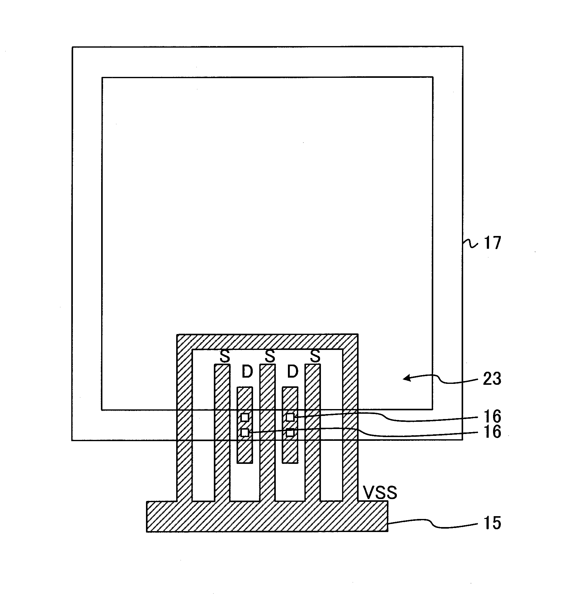
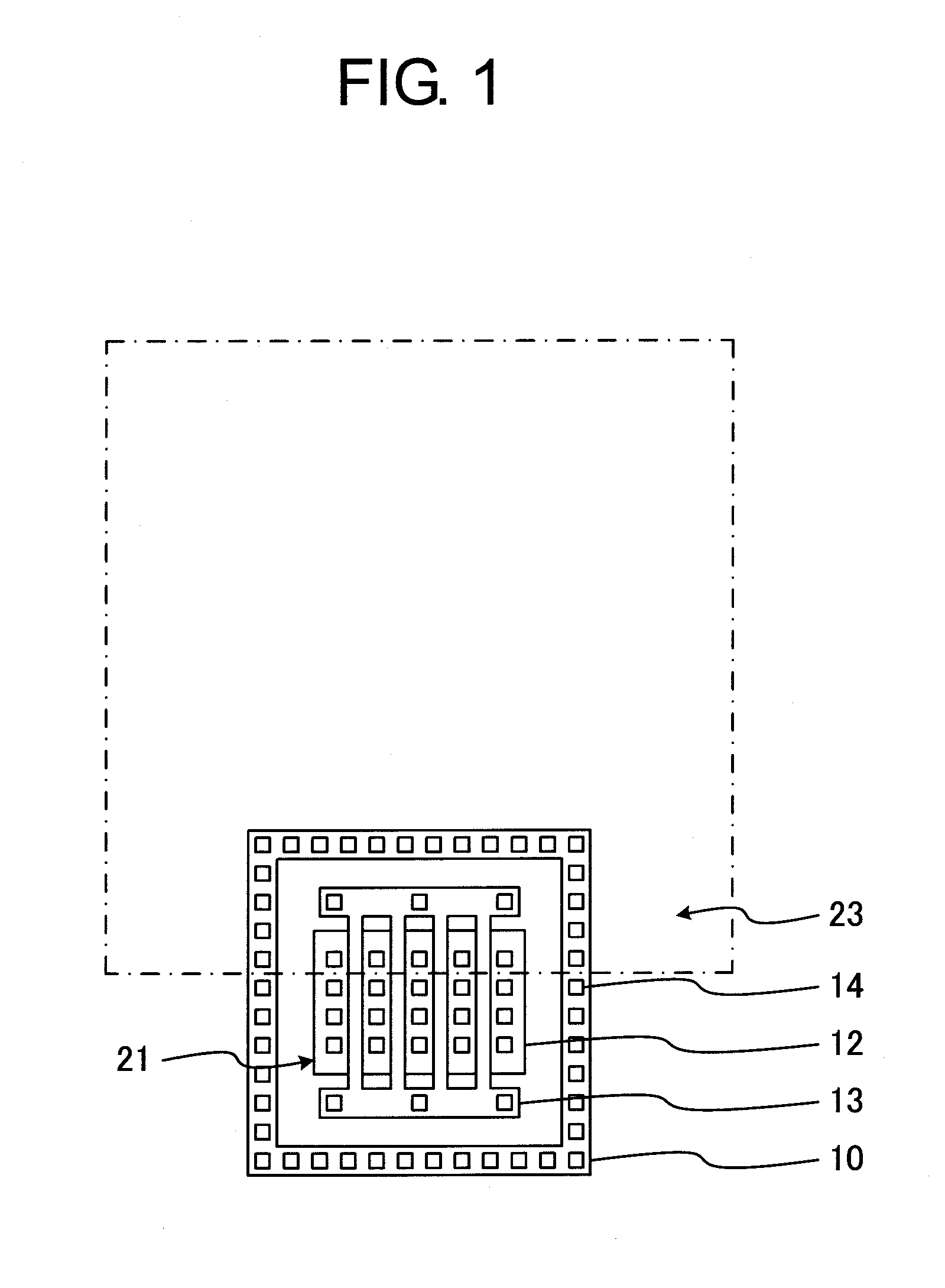
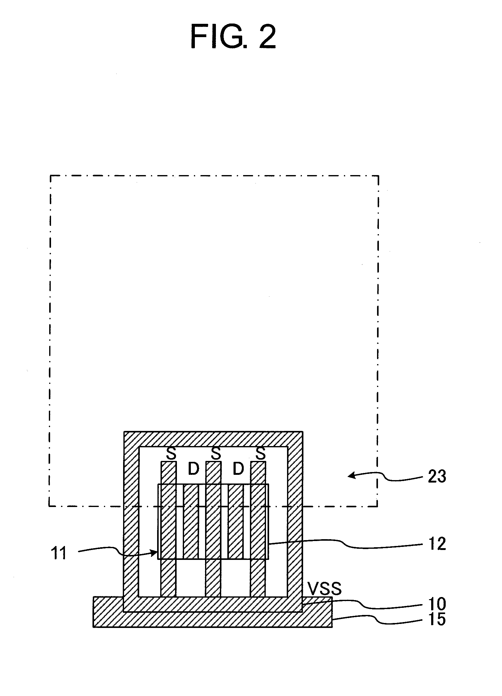
[0023]First, a pad structure of a semiconductor device according to the present invention is described with reference to plan views of FIGS. 1 to 4, which illustrate the pad structure of the semiconductor device. FIG. 1 illustrates diffusion regions, a gate electrode, a contact, and a pad opening. FIG. 2 illustrates the diffusion regions, a lower metal film, and the pad opening. FIG. 3 illustrates the lower metal film, a first via, an intermediate metal film, and the pad opening. FIG. 4 illustrates a second via, an upper metal film, and the pad opening.
[0024]As illustrated in FIG. 1, a gate electrode 13, a P-type diffusion region 10 for fixing a substrate potential, and an N-type diffusion region 12 for a source and a drain are arranged so as to overlap with an edge of a pad opening 23, to thereby construct an NMOS transistor 21. The NMOS transistor 21 is a multi-finger transistor, which is surrounded by the P-type diffusion region 10, and includes the N-type diffusion regions 12 fo...
second embodiment
[0035]FIG. 6 illustrates the present invention. FIG. 6 illustrates a diffusion region, a gate electrode, a contact, and a pad opening. In the case where the NMOS transistor 21 has the source regions at both ends and at the center, in order to stabilize a substrate potential in the vicinity of the source and drain regions, the P-type diffusion region 10 for fixing the substrate potential can be arranged along the center of the NMOS transistor 21 so as to be adjacent to the N-type diffusion region 12 for the source.
third embodiment
[0036]FIG. 7 illustrates the present invention. FIG. 7 illustrates a diffusion region, a gate electrode, a contact, and a pad opening. Although the NMOS transistor 21 of FIG. 1 includes the N-type diffusion region 12 serving as the source as a diffusion region at the end in the gate length direction, the NMOS transistor 21 may include an N-type diffusion region 12 serving as the drain as illustrated in FIG. 7. In FIG. 7, the location of the N-type diffusion region 12 for the source is changed, and along therewith, the location of the contact 14 on the gate electrode 13 is also changed.
[0037]As illustrated in FIG. 8, two NMOS transistors 21 may be arranged so as to be opposed to each other. In this case, the first via 16 for one of the NMOS transistors 21 is arranged on one side of the intermediate metal film 17, and the first via 16 for the other of the NMOS transistors 21 is arranged on another side thereof opposed to the one side. In this manner, the symmetry is ensured.
[0038]As i...
PUM
 Abstract
Description
Claims
Application Information