

Semiconductor device
a technology of semiconductor devices and circuits, applied in emergency protective circuits, emergency protective arrangements for limiting excess voltage/current, emergency protective arrangements, etc., can solve problems such as the configuration of semiconductor devices, and achieve high withstand voltage, improve the response speed of current, and increase the withstand voltage of current driving output terminals
- Summary
- Abstract
- Description
- Claims
- Application Information
AI Technical Summary
Benefits of technology
Problems solved by technology
Method used
Image

Examples
first embodiment
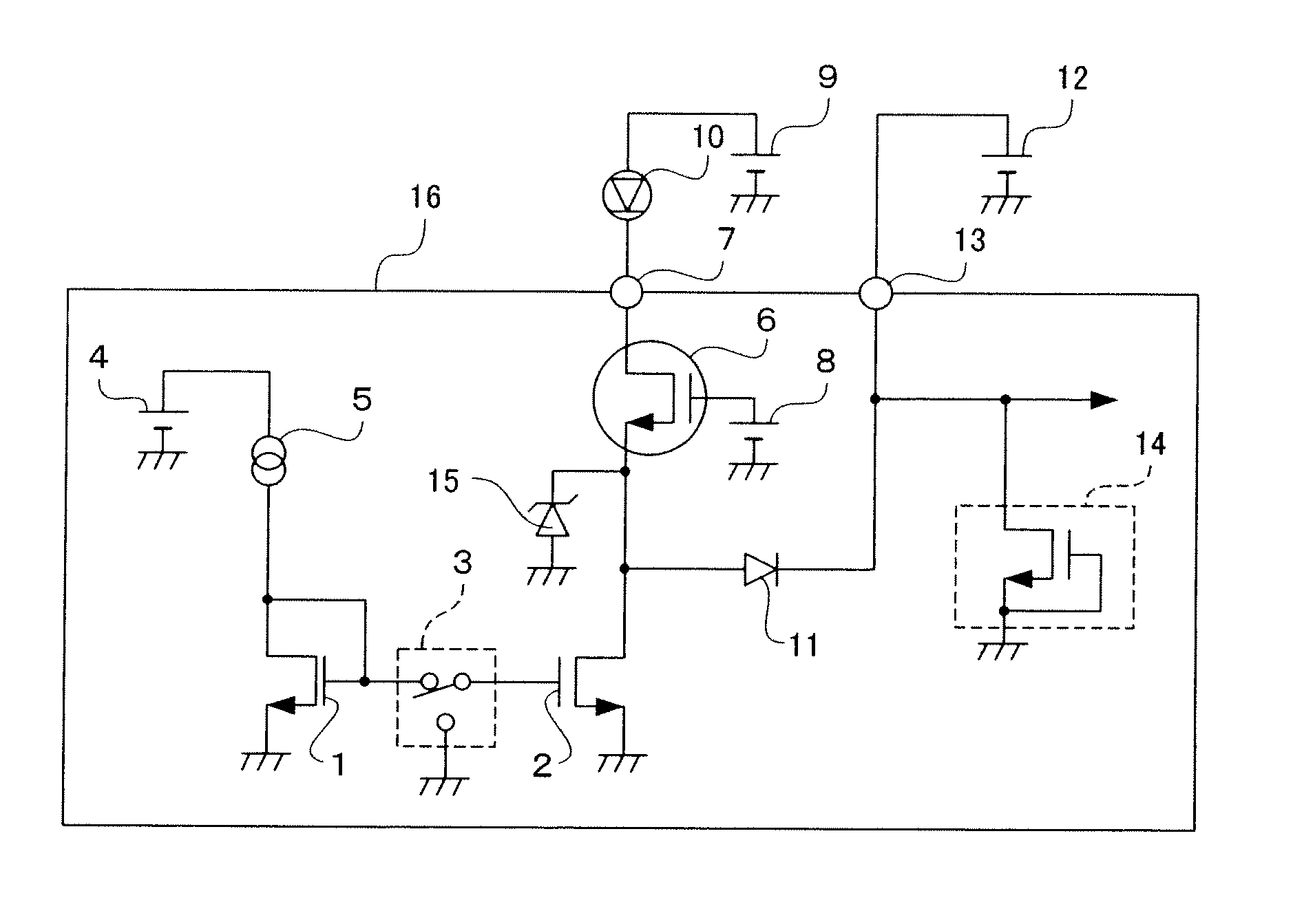
[0039]Referring to FIG. 1, the following will describe a semiconductor device according to a first embodiment of the present invention. FIG. 1 shows the schematic configuration of the main part of the semiconductor device according to the first embodiment of the present invention.
[0040]A switch circuit 3 is connected between a gate serving as the control terminal of an N-channel MOS transistor 1 and a gate serving as the control terminal of an N-channel MOS transistor 2. The N-channel MOS transistors 1 and 2 compose a current mirror circuit when the switch circuit 3 is turned on.
[0041]A drain serving as the input terminal of the N-channel MOS transistor 1 is connected to a constant current source 5. A constant voltage source 4 acts as the current supply source of the constant current source 5. A source serving as the output terminal of the N-channel MOS transistor 1 is grounded. A drain serving as the input terminal of the N-channel MOS transistor 2 is connected to a source serving ...
second embodiment
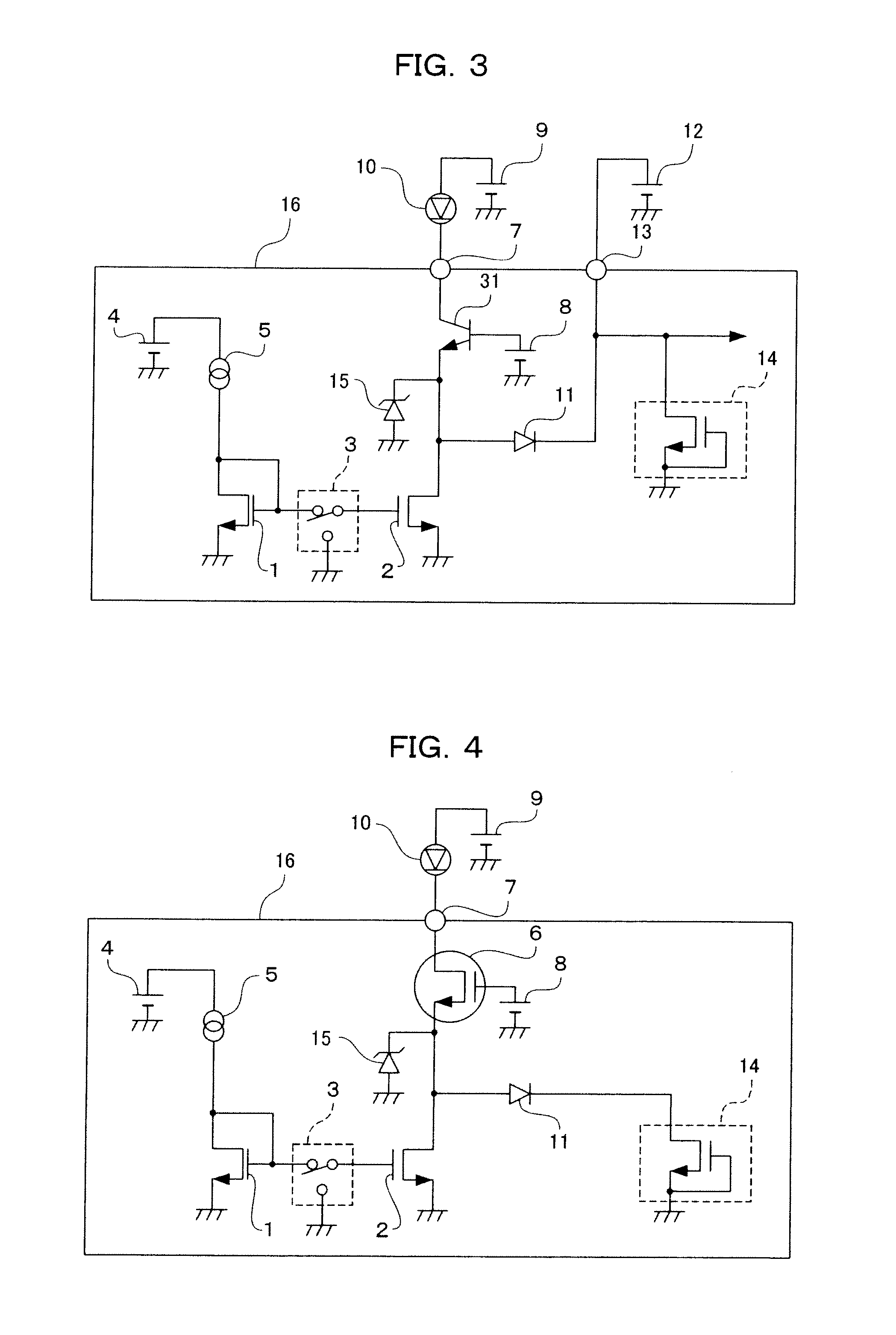
[0063]Referring to FIG. 3, the following will describe a semiconductor device according to a second embodiment of the present invention. Members corresponding to the members described in the first embodiment will be indicated by the same reference numerals and the explanation thereof is omitted.
[0064]FIG. 3 shows the schematic configuration of the main part of the semiconductor device according to the second embodiment of the present invention. As shown in FIG. 3, the semiconductor device is different from the semiconductor device of the first embodiment in that an NPN bipolar transistor 31 is used as a high withstand voltage cascode transistor connected to an output terminal 7. Hereinafter, the NPN bipolar transistor 31 will be simply referred to as the NPN transistor 31.
[0065]As in the first embodiment, the base voltage of the NPN transistor 31 is set such that the emitter voltage of the NPN transistor 31 is equal to or lower than the drain withstand voltage of an N-channel MOS tr...
third embodiment
[0067]Referring to FIG. 4, the following will describe a semiconductor device according to a third embodiment of the present invention. Members corresponding to the members described in the first embodiment will be indicated by the same reference numerals and the explanation thereof is omitted.
[0068]FIG. 4 shows the schematic configuration of the main part of the semiconductor device according to the third embodiment of the present invention. As shown in FIG. 4, the semiconductor device is different from the semiconductor device of the first embodiment in that the cathode of a diode 11 is in contact only with an ESD protection circuit 14.
[0069]According to the semiconductor device, the ESD protection circuit cannot be shared by an LED driving output terminal and a power supply input terminal unlike in the first embodiment. However, the ESD protection circuit 14 can be disposed with higher flexibility which reduces restrictions on layout. Thus it is possible to reduce a wiring impeda...
PUM
 Abstract
Description
Claims
Application Information