Semiconductor device, substrate for electro-optical device, electro-optical device, electronic device and projection display

Inactive Publication Date: 2002-02-12
SEIKO EPSON CORP
View PDF6 Cites 83 Cited by
  • Summary
  • Abstract
  • Description
  • Claims
  • Application Information

AI Technical Summary

Problems solved by technology

In the thin-film structure of the MOSFET, a diversity of problems arise, for example, an excess carrier (charge) lowers the breakdo

Method used


Image

  • Semiconductor device, substrate for electro-optical device, electro-optical device, electronic device and projection display
  • Semiconductor device, substrate for electro-optical device, electro-optical device, electronic device and projection display
  • Semiconductor device, substrate for electro-optical device, electro-optical device, electronic device and projection display

Examples


first embodiment

(First Embodiment)

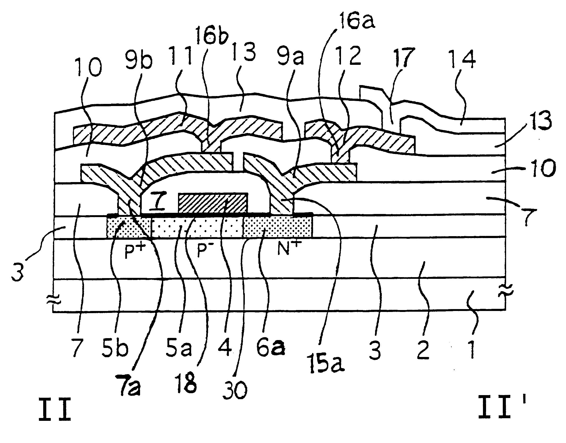
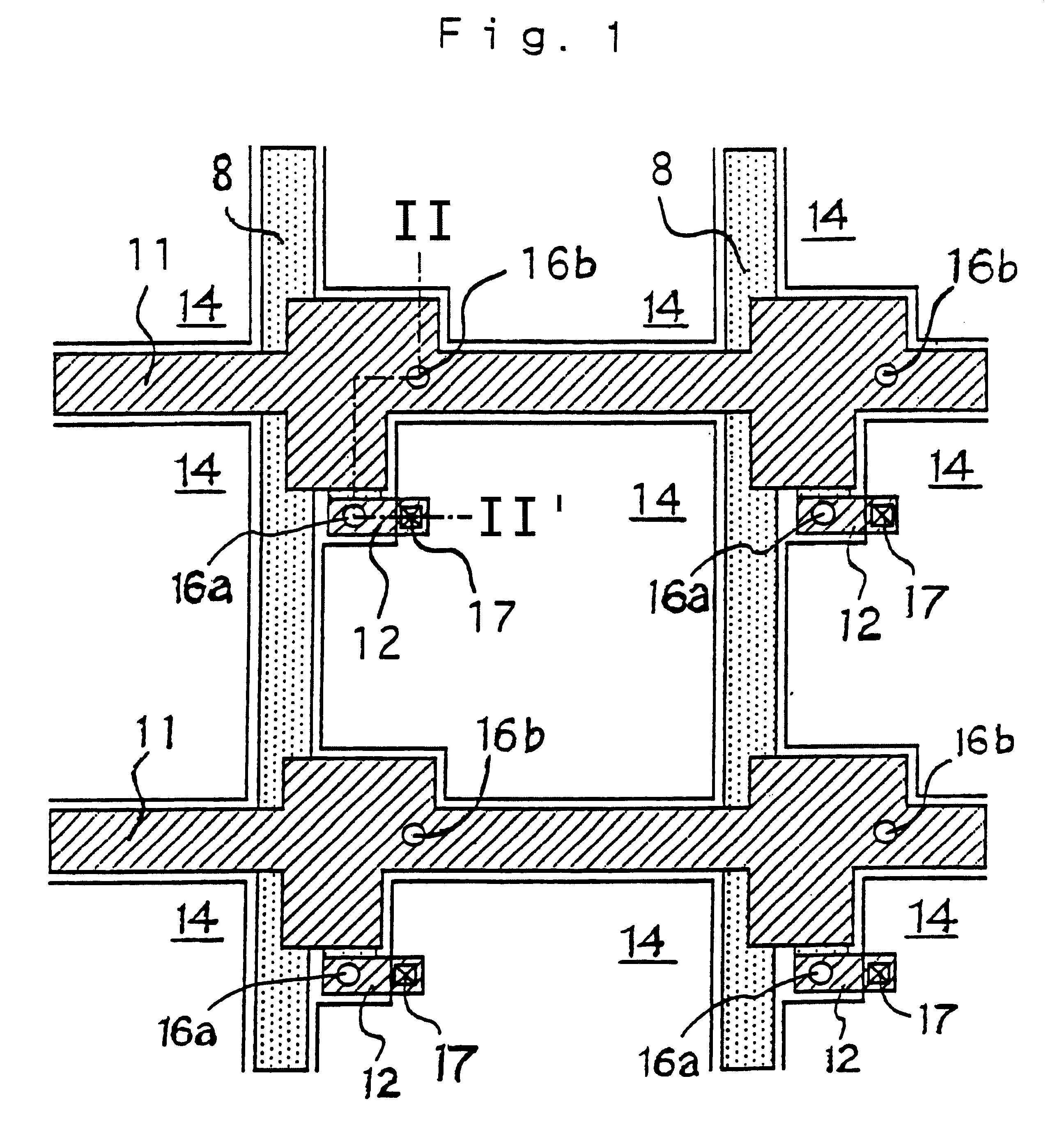
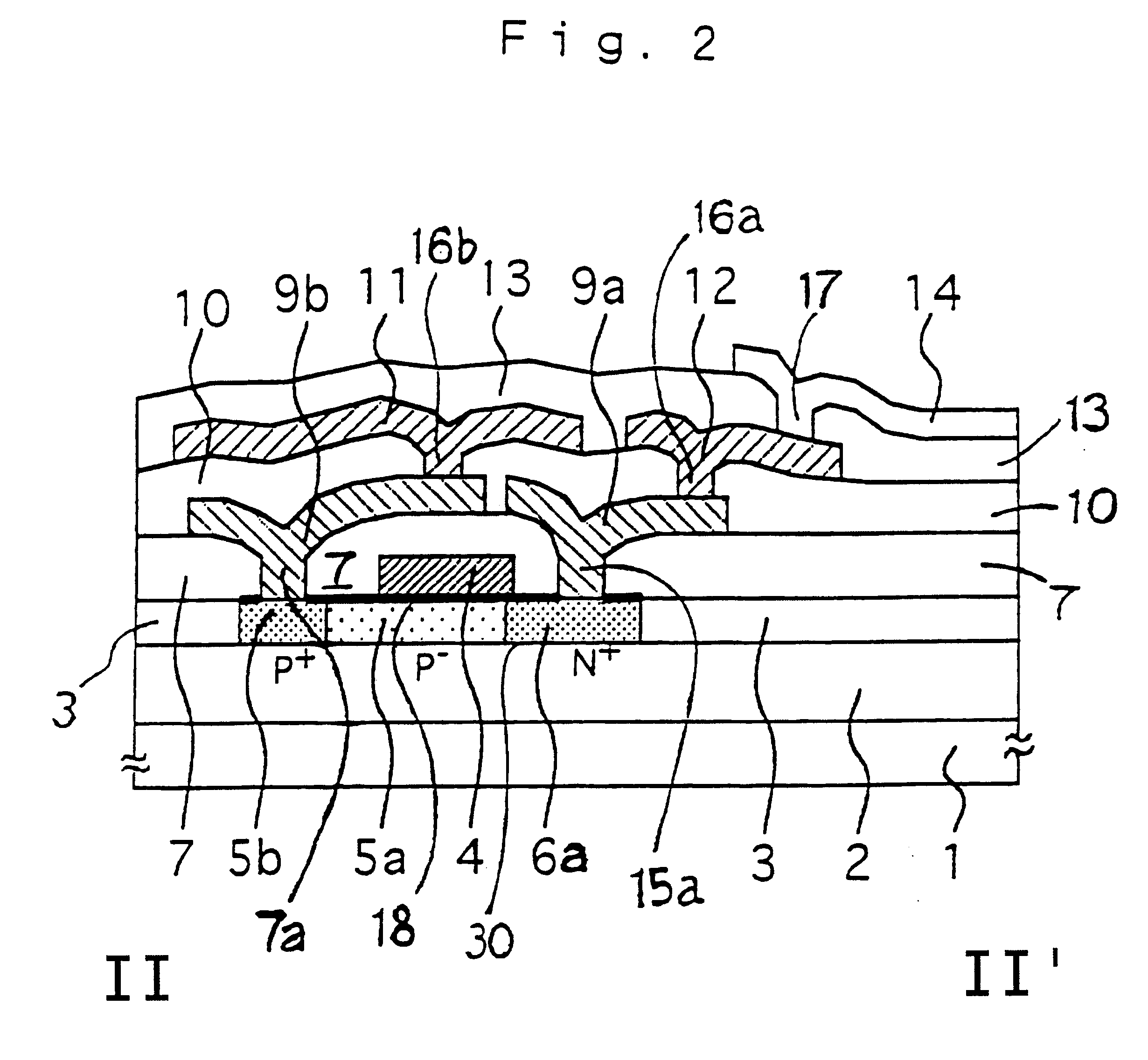
A first embodiment is a liquid-crystal display panel as one example of the substrate of an electro-optical device. This embodiment is discussed in connection with the substrate of the electro-optical device employing an SOI substrate in which a semiconductor layer is formed on an insulator. In each of the following embodiments, the substrate of the electro-optical device having a MOSFET formed on an insulator is discussed as one example of a semiconductor device of the present invention.

FIG. 1 is a plan view showing the layout of each layer in a pixel area in the liquid-crystal panel substrate of this embodiment. FIG. 3 is a plan view showing the layout of a semiconductor layer (monocrystalline silicon layer) in the pixel area in the liquid-crystal panel of this embodiment. FIG. 4 is a plan view showing the layout of the semiconductor layer (monocrystalline silicon layer), a polycrystalline silicon layer and an aluminum layer, in the pixel area in the liquid-crysta...

second embodiment

(Second Embodiment)

In a second embodiment, as one example of the substrate of the electro-optical device of the present invention, a light shielding layer 20 is added to the construction of the first embodiment in connection with the liquid-crystal panel. In this embodiment, same numerals, already quoted in the discussion of the first embodiment represent layers manufactured at the same steps or members having identical functions unless otherwise particularly noted. The second embodiment is now discussed. Like the first embodiment, the second embodiment employs an SOI substrate as a substrate for an electro-optical device in which a semiconductor layer is formed on an insulator.

FIG. 7 is a cross-sectional view of a pixel area of the liquid-crystal panel substrate of this embodiment. FIG. 8 shows the layout of a first light shielding layer and a semiconductor layer (monocrystalline silicon layer) in the pixel area of the liquid-crystal panel substrate of this embodiment. In this embo...


PUM


Abstract

The potential at a channel region of a MOSFET on a substrate needs to be stabilized to assure a drain withstand voltage. To this end, a new potential line is additionally required. However, the addition of the potential line causes a drop in the aperture ratio in a transmissive type liquid-crystal display device, in which lightness is particularly important. A light shielding layer overlapping the MOSFET formed on the substrate is electrically connected to the channel region in the MOSFET.

Description

1. Field of the InventionThe present invention relates to a semiconductor device, a substrate for an electro-optical device, the electro-optical device, an electronic equipment, and a projector.2. Description of Related ArtThe SOI (Silicon On Insulator) technology in which a semiconductor device is formed on a silicon insulator film on top of an insulating substrate has been extensively studied because the SOI technologies offer high-speed, low-power consumption features and the high degree of integration in devices.One of the SOI technologies is a manufacturing technique of an SOI substrate in which monocrystalline silicon substrates are laminated. In this method, called a lamination technique, after a monocrystalline silicon substrate and a support substrate are laminated using hydrogen bond force, the strength of the lamination is reinforced by a thermal treatment, and the monocrystalline silicon substrate is subjected to grinding and abrasion or a thin-film monocrystalline silic...

Claims


Application Information

Patent Timeline
IPC IPC(8): G02F1/13G02F1/1362H01L29/66H01L29/786G02F1/1368
CPCG02F1/136209H01L29/78633H01L29/78612G02F1/1368H01L21/18
Inventor KAWATA, HIROTAKA
Owner SEIKO EPSON CORP
Why Eureka
Try Eureka