
Electrostatic discharge protection circuit and deep submicron semiconductor component thereof

An electrostatic discharge protection and semiconductor technology, which is applied in the field of deep sub-micron semiconductor components, can solve the problems of weakening and shrinking of antistatic ability, and achieves strengthening electrostatic discharge tolerance, improving electrostatic discharge tolerance, and improving electrostatic discharge tolerance. force effect

Inactive Publication Date: 2018-06-29
ADVANCED ANALOG TECH INC
View PDF8 Cites 0 Cited by
  • Summary
  • Abstract
  • Description
  • Claims
  • Application Information

AI Technical Summary

Problems solved by technology

[0005] However, with the evolution of semiconductor technology, the components of integrated circuits have shrunk from micron to deep sub-micron (MOS gate width is less than 0.18um). Micron integrated circuit layout rules (VLSI layout rule) are relatively reduced, making the distance between the drain and source of the PMOS and NMOS components of the electrostatic discharge protection circuit too close, resulting in weakened antistatic capabilities; and because of the size of the PMOS and NMOS components Shrinking, electrostatic discharge current is easier to pass through the surface channels of PMOS and NMOS components, and burns PMOS and NMOS components

Method used


Image

  • Electrostatic discharge protection circuit and deep submicron semiconductor component thereof
  • Electrostatic discharge protection circuit and deep submicron semiconductor component thereof
  • Electrostatic discharge protection circuit and deep submicron semiconductor component thereof

Examples


Embodiment Construction

[0049] The present invention is aimed at improving the electrostatic discharge tolerance of deep submicron components used for electrostatic discharge protection. Hereinafter, a number of embodiments are used to specifically illustrate the technical content of the present invention.

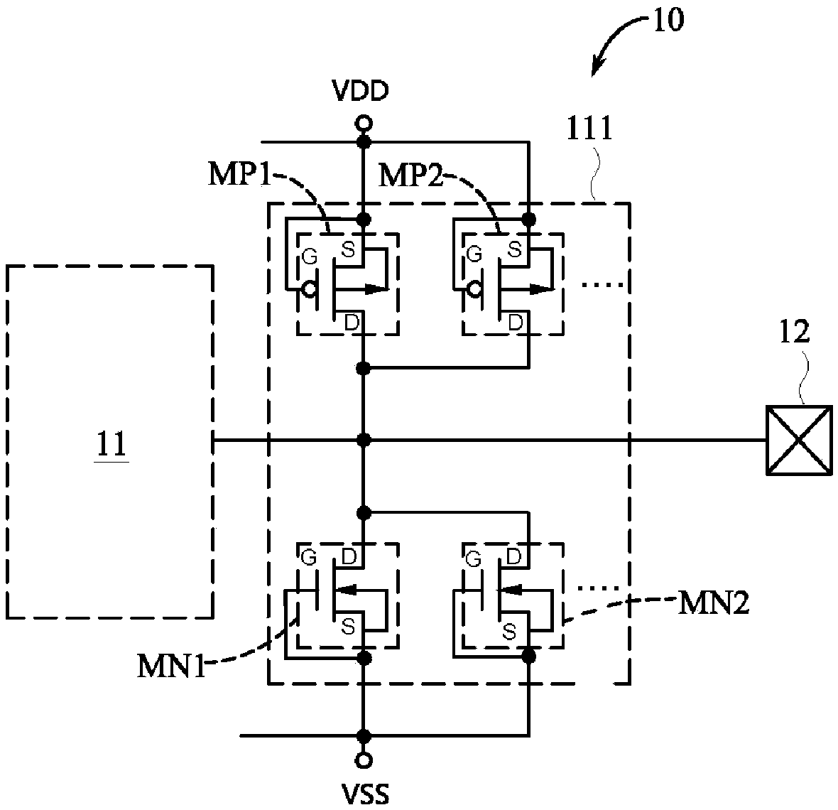
[0050] See first figure 1 As shown, the electrostatic discharge protection circuit 111 of the present invention includes a plurality of parallel PMOS elements MP1, MP2 and a plurality of parallel NMOS elements MN1, MN2 connected in series with each other, and the series connection node is connected to an input / output pad 12 of an integrated circuit 10 and An internal circuit 11; wherein the gate G and source S of each PMOS element MP1, MP2 are commonly connected to the high potential VDD of the system power supply of the integrated circuit 10, and the gate G and source S of each NMOS element MN1, MN2 Commonly connected to the low potential VSS of the system power supply of the integrated circuit 10....


PUM


Abstract

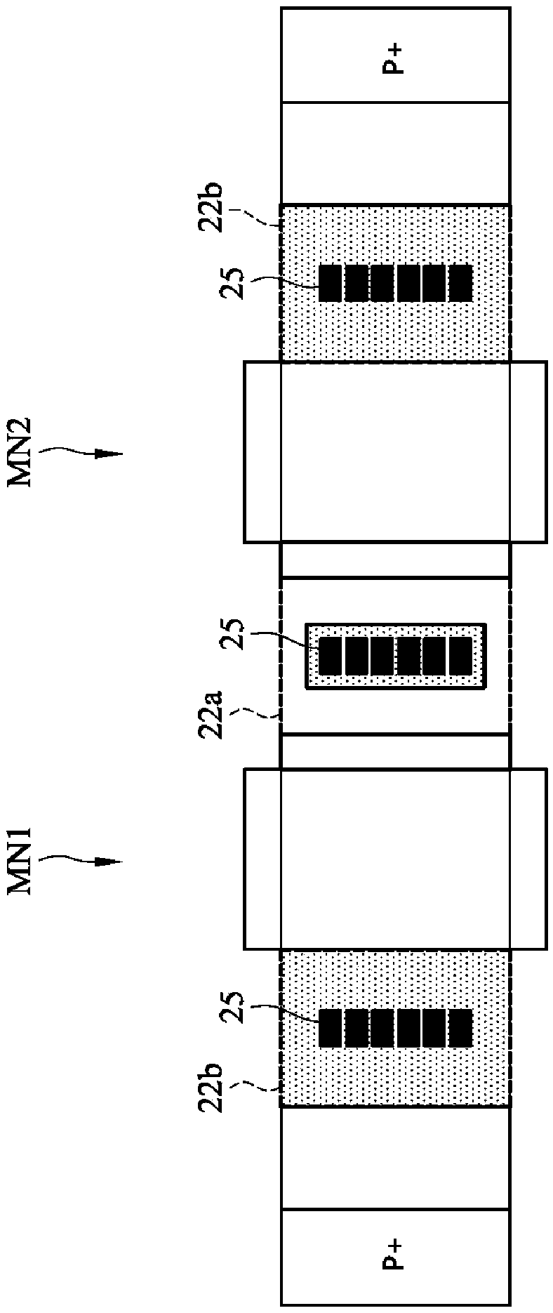
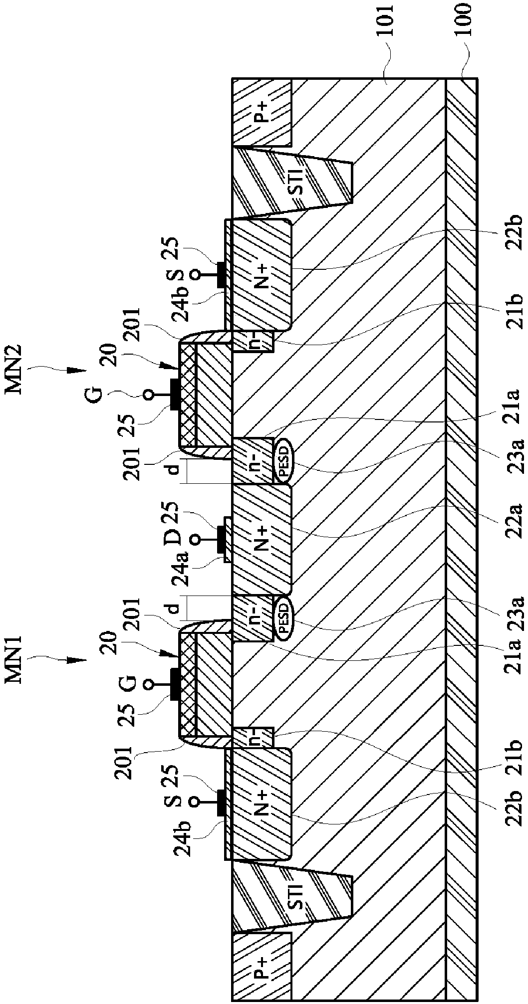
The invention discloses an electrostatic discharge protection circuit and a deep submicron semiconductor component thereof. A boundary between a heavily doped region corresponding to a drain electrodeof the deep submicron semiconductor component and an adjacent lightly doped region are pushed outwardly, so that a gap is formed between the boundary and the sidewall of the nearest grid insulating layer and the boundary is not aligned with the sidewall of the grid insulating layer. Thus, in the deep submicron semiconductor component, the drain electrode is not too close to a source electrode dueto smaller layout of a deep submicron technology, and the electrostatic discharge tolerance of the deep submicron semiconductor component is improved effectively.

Description

Technical field [0001] The invention relates to a deep submicron semiconductor element, in particular to a deep submicron semiconductor element protected by electrostatic discharge. Background technique [0002] Since the internal components of integrated circuits are easily damaged by electrostatic discharge, electrostatic discharge protection engineering is particularly important for integrated circuits. See Image 6 As shown, since static electricity is easily discharged through the input / output pads 52 of the integrated circuit 50 to its internal components 51, an electrostatic discharge protection circuit 511 is provided on each input / output pad 52, which mainly includes a PMOS connected in series. (P-type metal-oxide-semiconductor element MP and an NMOS (N-type metal-oxide-semiconductor) element MN; wherein the series connection node of the PMOS element MP and the NMOS element MN is connected to the corresponding input / output pad 52, and The gate G and the source S of the P...

Claims


Application Information

Patent Timeline
IPC IPC(8): H01L27/02
CPCH01L27/0207H01L27/0266
Inventor 林欣逸谢协缙
Owner ADVANCED ANALOG TECH INC
Learn More