

ESD protection component layout structure with high ESD tolerance
A technology of electrostatic protection and layout structure, which is applied in the direction of electrical components, electric solid devices, circuits, etc., can solve the problems of inability to provide electrostatic tolerance and easy burning, and achieve improved electrostatic current, improved electrostatic discharge tolerance, and reduced Effect of Substrate Resistance
- Summary
- Abstract
- Description
- Claims
- Application Information
AI Technical Summary
Problems solved by technology
Method used
Image

Examples
Embodiment Construction
[0036] The present invention will be described in detail below in conjunction with the accompanying drawings and specific embodiments, but not as a limitation of the present invention.
[0037] The present invention proposes improvements to the electrostatic discharge tolerance of integrated circuit electrostatic protection components, and in particular improves the electrostatic protection components composed of NMOS transistors to enhance their electrostatic discharge tolerance. In the following, several embodiments will be described in detail in conjunction with the drawings.
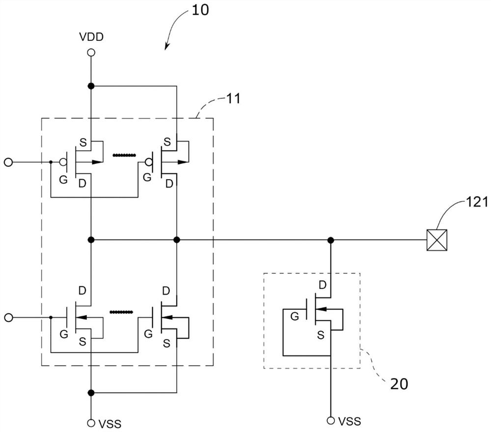
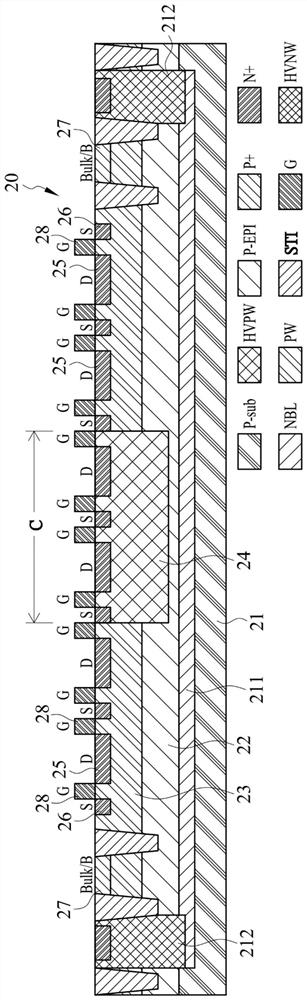
[0038] See first figure 1 Shown is the layout structure of an electrostatic protection element of the present invention. In this embodiment, the electrostatic protection element is an NMOS transistor element 20; please cooperate Figure 2A As shown, the NMOS transistor element 20 includes a P-type substrate 21, a first P-type doped region 22, a P-type well 23, a second P-type doped region 24, a plu...
PUM
 Abstract
Description
Claims
Application Information