Semiconductor light emitting element
A light-emitting element and semiconductor technology, applied in semiconductor devices, electrical components, circuits, etc., can solve problems such as asymmetric distribution of electrons and holes, achieve the effects of improving luminous efficiency, avoiding lattice quality, and increasing luminous intensity
- Summary
- Abstract
- Description
- Claims
- Application Information
AI Technical Summary
Problems solved by technology
Method used
Image
Examples
Embodiment 1
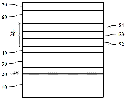
[0032] See attached figure 1 , a semiconductor element with a composite structure layer 50, comprising a substrate 10, and a nitride buffer layer 20, an n-type layer 30, a shallow quantum well layer 40, a multi-quantum well layer 60 and a p-type layer sequentially formed on the substrate 10 layer 70, and a composite structure layer 50 located between the shallow quantum well layer 40 and the multiple quantum well layer 60, wherein the substrate 10 is a sapphire flat substrate, a sapphire patterned substrate, a silicon nitride substrate, a GaN substrate , silicon substrate, glass substrate or metal substrate, the nitride buffer layer 20 is a single-layer structure or a superlattice structure, which is a binary or ternary structure composed of Ga, N, In, Al Or a quaternary structure; the p-type layer 70 is a Mg-doped GaN layer.
[0033] Continue to see attached figure 1 , in this embodiment, the composite structure layer 50 at least includes a p-type doped GaN layer 54, an n-t...
Embodiment 2
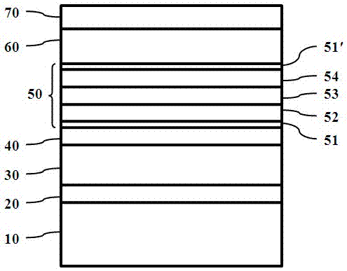
[0036] See attached figure 2 Compared with Embodiment 1, this embodiment differs in that the composite structure layer 50 further includes a first electron blocking layer 51 located at its lower end and a second electron blocking layer 51' located at its upper end. , wherein the materials of the first electron blocking layer 51 and the second electron blocking layer 51' are both AlGaN, and their thicknesses are the same or different. In this embodiment, the thickness of the electron blocking layer 51 and the second electron blocking layer 51' is preferably the same, preferably The thickness range is 400 angstroms to 600 angstroms.
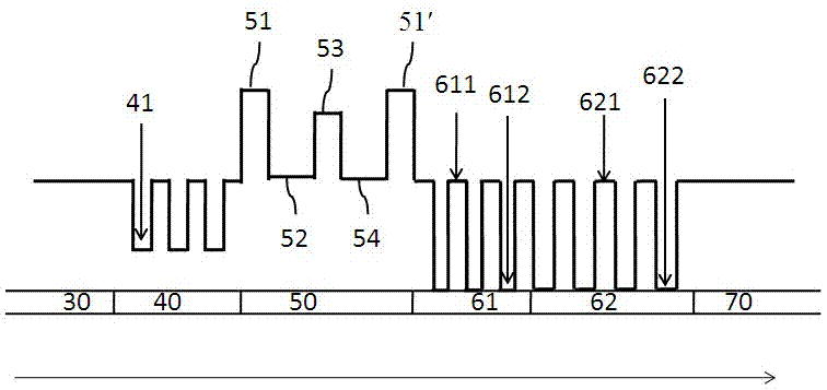
[0037] Specifically, see the attached image 3, the composite structure layer 50 from bottom to top is the first electron blocking layer 51, n-type doped GaN layer 52, Al x In y Ga 1-x-y N isolation layer 53, p-type doped GaN layer 54, and second electron blocking layer 51'; wherein, the band gap of isolation layer 53 is greater than that of p...
Embodiment 3
[0042] See attached Figure 4 The difference between this embodiment and Embodiment 1 is that the composite structure layer 50 includes a p-type doped GaN layer 54, an n-type doped GaN layer 52, and a p-type doped GaN layer 54 and an n-type doped GaN layer. The material between 52 is Al x In y Ga 1-x- y The periodic structure 50' composed of N isolation layers 53 alternately, the first electron blocking layer 51 located at the lower end of the composite structure layer 50, and the second electron blocking layer 51' located at the upper end of the composite structure layer 50, wherein the periodic structure 50' The number of cycles is greater than or equal to 2, and each cycle includes an n-type doped GaN layer 52, an isolation layer 53, a p-type doped GaN layer 54, and an isolation layer 53, and the first electron blocking layer 51 and the second electron blocking layer 51' are in the While enriching the electrons in the composite structure layer 50, control the migration ...
PUM
 Abstract
Description
Claims
Application Information


