Process for manufacturing AlGaInP light-emitting diode with inclined side face

A technology of light-emitting diodes and aluminum gallium indium phosphide, which is applied to electrical components, circuits, semiconductor devices, etc., can solve the problems of poor heat dissipation and low light extraction efficiency of light-emitting diodes, and achieve the expansion of the range of light output angles, the increase of light output areas, and the light output. The effect of improving efficiency

Inactive Publication Date: 2010-08-18
XIAMEN SANAN OPTOELECTRONICS TECH CO LTD
View PDF4 Cites 19 Cited by
  • Summary
  • Abstract
  • Description
  • Claims
  • Application Information

AI Technical Summary

Problems solved by technology

The top surface of the light-emitting diode is planar, and the bottom surface of the substrate opposite to it is parallel to each other. As we all know, light is incident from an optically dense medium into an optically sparse medium. If the incident angle of light is outside the critical angle, That is to say, there will be an unexpected phenomenon, which is the internal total reflection phenomenon. Since the two opposite sides of the above-mentioned light-emitting diode are parallel planes, the photons are affected by total reflection, and the light extraction efficiency becomes low. At the same time, the photons are limited to the light-emitting diode. In the chip, these photons cannot escape smoothly from the light-emitting diode chip to the outside air, so the heat dissipation of the light-emitting diode is poor

Method used


Image

  • Process for manufacturing AlGaInP light-emitting diode with inclined side face
  • Process for manufacturing AlGaInP light-emitting diode with inclined side face
  • Process for manufacturing AlGaInP light-emitting diode with inclined side face

Examples


Embodiment Construction

[0023] The present invention will be further described below in conjunction with the accompanying drawings and embodiments.

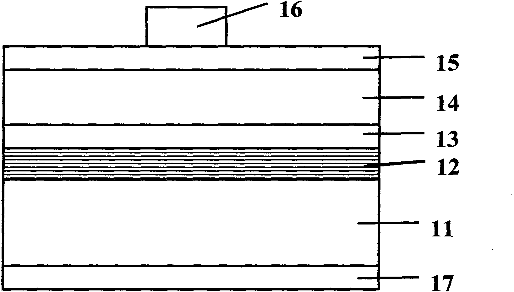
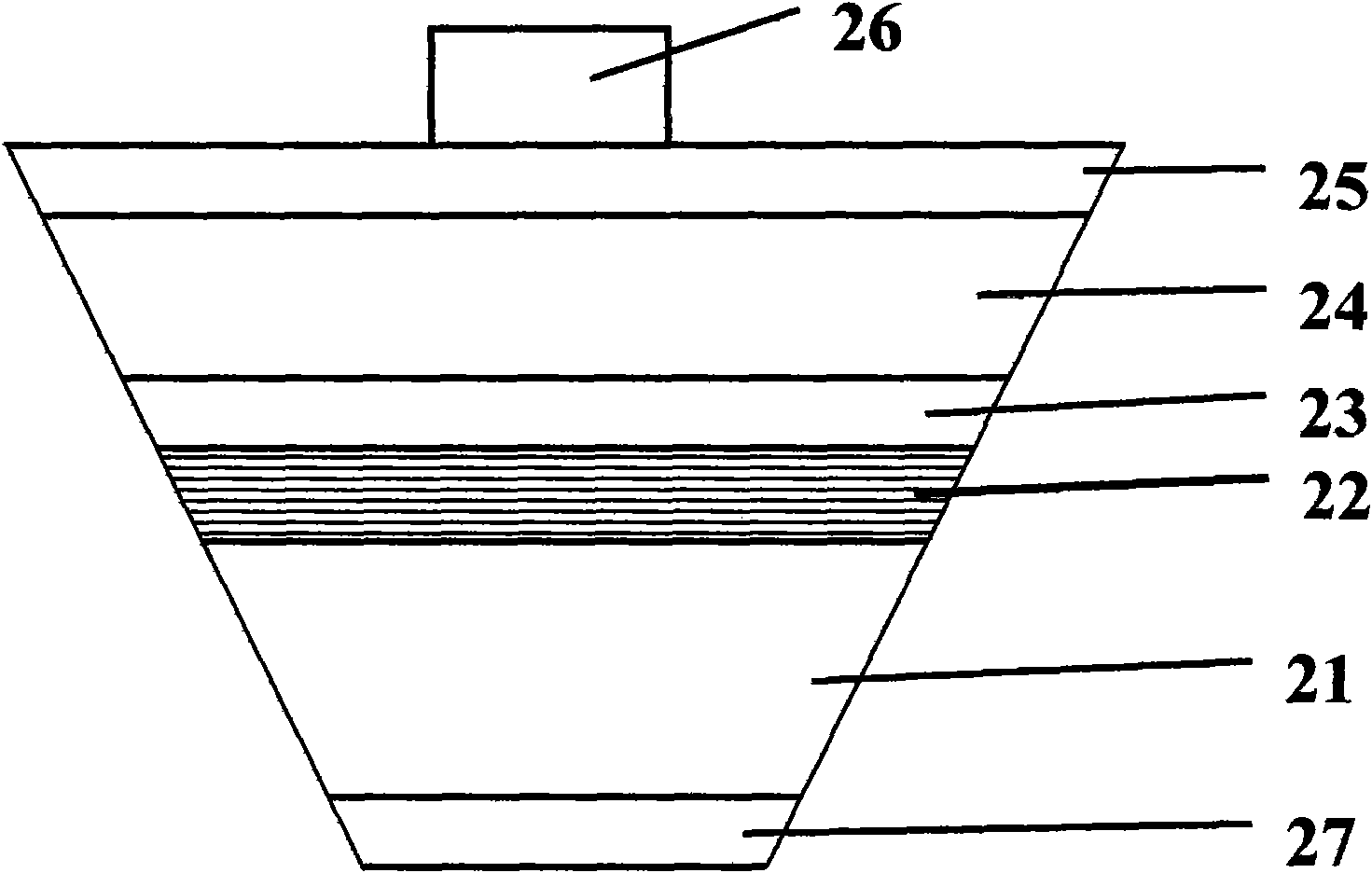
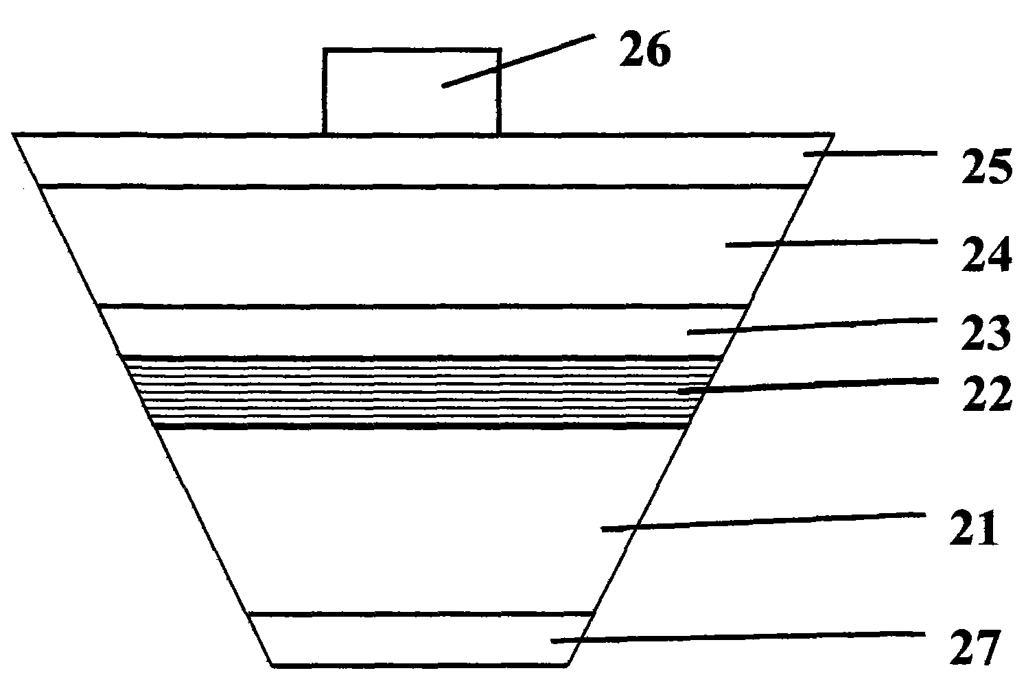
[0024] figure 2 As shown, a manufacturing method of laser lift-off GaN-based light-emitting devices using the synthetic separation method provides a gallium arsenide substrate 21; a distributed Bragg reflection layer 22 is formed on the top surface of the gallium arsenide substrate 21, and the distributed Bragg reflection layer 22 is composed of stacked material layers with alternating high and low refractive index; a first-type epitaxial layer 23 is formed on the distributed Bragg reflection layer 22; a light-emitting layer 24 is formed on the top surface of the first-type epitaxial layer 23; The second-type epitaxial layer 25; the P electrode 26 is formed on the top surface of the second-type epitaxial layer 24; the N electrode 27 is formed on the bottom surface of the gallium arsenide substrate 21 to form an LED chip; an inductively coupled plasma d...


PUM


Abstract

The invention discloses a process for manufacturing a AlGaInP light-emitting diode with an inclined side face, which comprises the following steps: providing a substrate, forming a distributed Bragg reflecting layer on the top of the substrate, forming a first type epitaxial layer on the distributed Bragg reflecting layer, forming a luminous layer on the first type epitaxial layer, and forming a second type epitaxial layer on the luminous layer; forming a P electrode on the second type epitaxial layer, and forming an N electrode at the bottom surface of the substrate to form an LED chip; cutting the side face of the LED chip at an inclination angle along the direction from the top to the bottom surface of the LED chip by adopting a dry etching method, and cutting the bottom surface of the LED chip by using laser; and finally, cutting through the side face at the bottom of the LED chip by using a diamond knife and forming an inclined plane at the periphery of the LED chip. The AlGaInP light-emitting diode has the advantages of increasing emergent light and decreasing light refracting or reflecting frequency to improve luminous efficiency, and the like.

Description

technical field [0001] The invention relates to a manufacturing process of a quaternary light-emitting diode, in particular to a manufacturing process of an aluminum gallium indium phosphorus light-emitting diode with inclined sides. Background technique [0002] Light Emitting Diode (English for Light Emitting Diode, referred to as LED) is a semiconductor diode, it can convert electrical energy into light energy, emit yellow, green, blue and other colors of visible light and infrared and ultraviolet invisible light; and small incandescent Compared with bulbs and neon lamps, it has the advantages of low working voltage and current, high reliability, long life and convenient adjustment of luminous brightness. [0003] In 1962, the world's first commercial red gallium arsenide phosphorous (GaAsP) light-emitting diode was successfully produced by General Electric Company, and the light-emitting diode began to show its position in the light-emitting device market. In the early ...

Claims


Application Information

Patent Timeline
Patent Type & Authority Applications(China)
IPC IPC(8): H01L33/20
Inventor 林素慧蔡家豪郑建森林科闯
Owner XIAMEN SANAN OPTOELECTRONICS TECH CO LTD
Why Eureka
Try Eureka