Semiconductor laser and manufacturing method thereof

A semiconductor and laser technology, applied in the field of mid-infrared semiconductor lasers, can solve the problems of high optical power density, optical catastrophe, inability to guarantee the operation of single transverse mode and single longitudinal mode, etc., and achieve the effect of high beam quality and high power output

Inactive Publication Date: 2015-12-16
INST OF SEMICONDUCTORS - CHINESE ACAD OF SCI
View PDF1 Cites 16 Cited by
  • Summary
  • Abstract
  • Description
  • Claims
  • Application Information

AI Technical Summary

Problems solved by technology

[0003] The common methods to achieve single longitudinal mode wavelength stabilization are DFB structure and DBR structure. For GaSb-based materials, the problem of easy oxidation caused by the high aluminum component in the waveguide layer and confinement layer makes the traditional burial method that requires secondary epitaxy. The production of grating DFB is very difficult
GaSb-based DFB uses the ridge waveguide and Bragg grating in the epitaxial layer to complete the refractive index guidance and gain guidance of light. However, in order to ensure the single-mode op...

Method used


Image

  • Semiconductor laser and manufacturing method thereof
  • Semiconductor laser and manufacturing method thereof
  • Semiconductor laser and manufacturing method thereof

Examples


Embodiment Construction

[0035] In order to make the object, technical solution and advantages of the present invention clearer, the present invention will be further described in detail below in conjunction with specific embodiments and with reference to the accompanying drawings.

[0036]It should be noted that implementations not shown or described in the accompanying drawings are forms known to those of ordinary skill in the art. Additionally, while illustrations of parameters including particular values ​​may be provided herein, it should be understood that the parameters need not be exactly equal to the corresponding values, but rather may approximate the corresponding values ​​within acceptable error margins or design constraints. In addition, the directional terms mentioned in the following embodiments only refer to the directions of the drawings. Accordingly, the directional terms are used to illustrate and not to limit the invention.

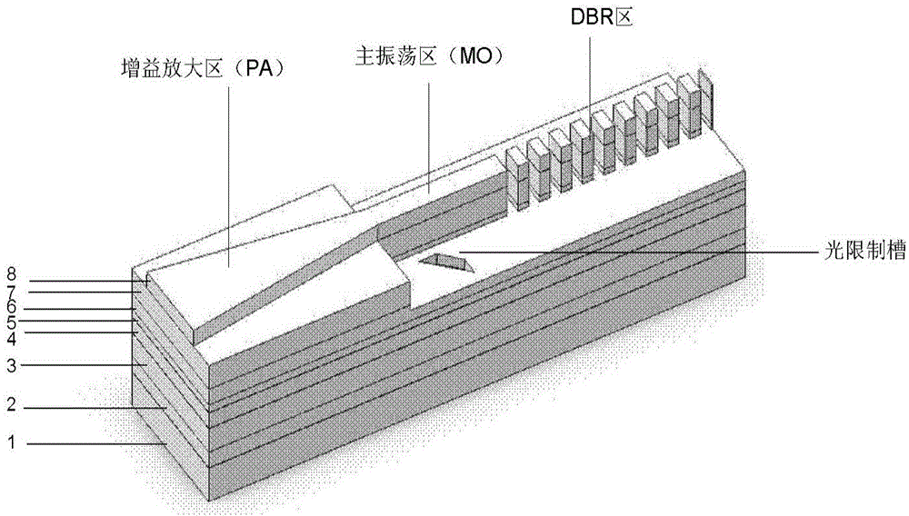
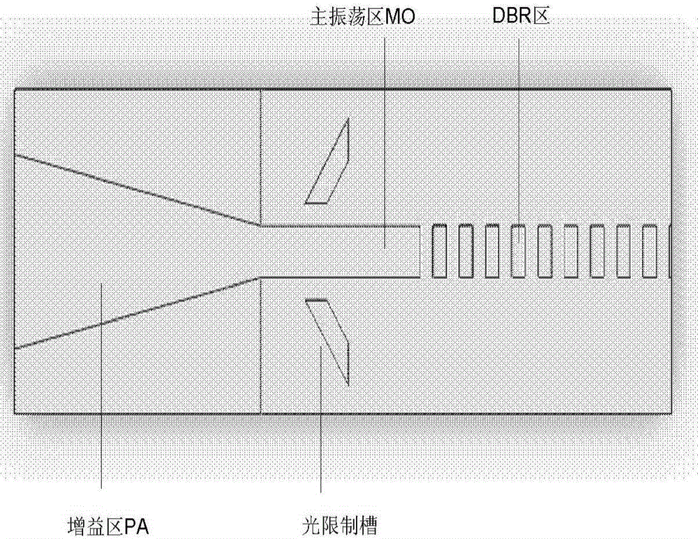
[0037] The invention provides a single-mode, high-power...


PUM

PropertyMeasurementUnit
Lengthaaaaaaaaaa
Etching depthaaaaaaaaaa
Cycleaaaaaaaaaa

Abstract

The invention discloses a single-mode high-power high-brightness GaSb-based bragg reflection master oscillator power amplifier (MOPA) integrated semiconductor laser and a manufacturing method thereof. The bragg reflection MOPA integrated semiconductor device comprises a substrate, an epitaxy structure, a gain amplification region, a master oscillator region, a bragg reflection region and optical limiting grooves, wherein the epitaxy structure grows on the substrate and comprises an N-type lower contact layer, an N-type lower limiting layer, a lower waveguide layer, an active region, an upper waveguide region, a P-type upper limiting layer and a P-type upper contact layer from bottom to top; the gain amplification region is located on the front part, namely a light outlet part, of the semiconductor laser, and is in a conical structure which is formed by etching the P-type upper contact layer downwards; the master oscillator region is located at the rear part of the gain amplification region and is in a ridge waveguide structure which is formed by etching the P-type upper limiting layer downwards; the bragg reflection region is located at the rear part of the master oscillator region and is in a periodical bragg grating structure which is formed by etching the P-type upper limiting layer downwards; and the optical limiting grooves are symmetrically distributed in two sides of the ridge waveguide and are obliquely arranged together with the ridge waveguide.

Description

technical field [0001] The invention relates to a mid-infrared semiconductor laser, in particular to a single-mode high-power high-brightness GaSb-based Bragg reflector MOPA integrated semiconductor laser and a preparation method thereof. Background technique [0002] The 2-5μm band contains a very important atmospheric window, including the characteristic spectral lines of many gas molecules, which can be widely used in civil projects such as air pollution monitoring and gas detection; and high-power lasers working in this band can be expected to be used in lidar, It can play a better application effect in military projects such as photoelectric countermeasures. Traditional Si-based and GaAs-based materials have relatively wide band gaps and cannot meet the requirements for wavelength. The relatively narrow bandgap of GaSb material has inherent advantages. However, most F-P cavity semiconductor lasers with common structures work in multimode, and spectral broadening effect...

Claims


Application Information

Patent Timeline
IPC IPC(8): H01S5/068H01S5/065H01S5/32
Inventor 杨成奥张宇廖永平魏思航徐应强牛智川
Owner INST OF SEMICONDUCTORS - CHINESE ACAD OF SCI
Why Eureka
Try Eureka