
Transistor capable of boosting electro-static discharge tolerance and its layout method

A technology of electrostatic discharge and layout method, which is applied in the direction of transistors, electric solid devices, circuits, etc., and can solve problems such as NSCR transistor 50 damage

Inactive Publication Date: 2009-09-23
ILI TECHNOLOGY CORPORATION
View PDF2 Cites 0 Cited by
  • Summary
  • Abstract
  • Description
  • Claims
  • Application Information

AI Technical Summary

Problems solved by technology

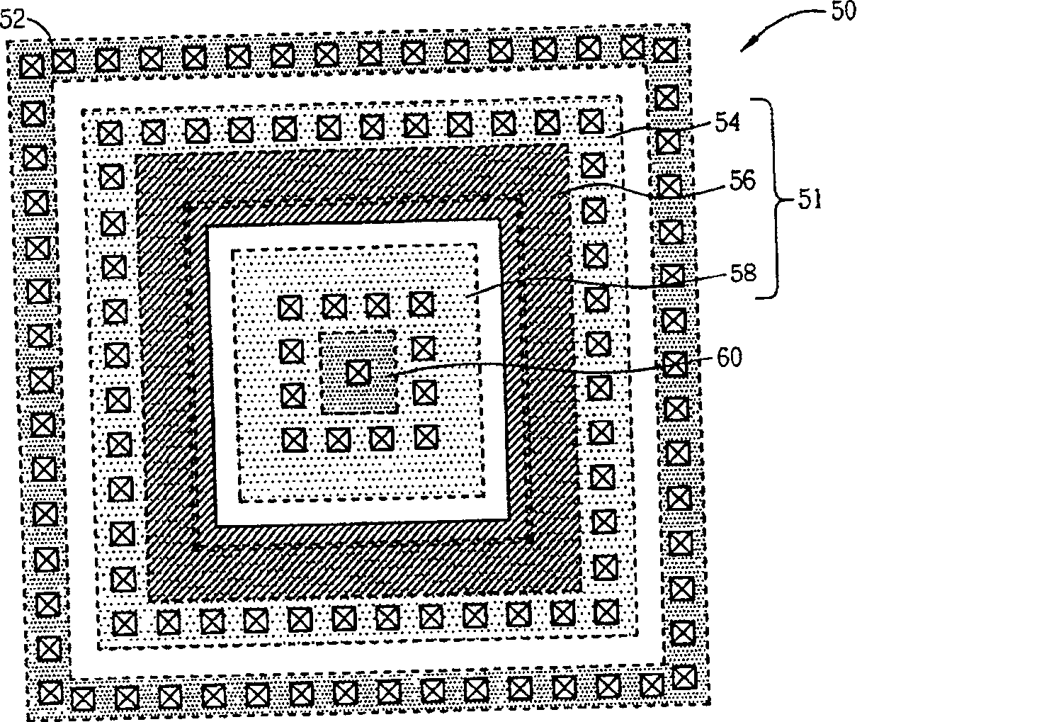
Please note that under this transistor layout, although the source and drain of the NMOS transistor 51 are far apart, the problem of the aforementioned NSCR transistor 10 can be solved, but the instantaneous large current input from the drain mainly flows through the P-type diffusion region 60 , if the area of ​​the P-type diffusion region 60 is too small, it may also cause damage to the NSCR transistor 50

Method used


Image

  • Transistor capable of boosting electro-static discharge tolerance and its layout method
  • Transistor capable of boosting electro-static discharge tolerance and its layout method
  • Transistor capable of boosting electro-static discharge tolerance and its layout method

Examples


Embodiment Construction

[0023] see Figure 4 , Figure 4 It is a schematic diagram of an embodiment of the NSCR transistor layout of the present invention. In this embodiment, the NSCR transistor 100 is a silicon-controlled rectifier (Silicon-Controlled Rectifiercell, SCR cell), which includes a Figure 4 The NMOS transistors 98A, 98B marked as 108, 112, 114, 104, and 106 are composed of a P-type semiconductor substrate (not shown), a P-type guard ring region 102, and two strip-shaped N-type diffusion Regions 104, 106, an annular N-type diffusion region 108, a P-type diffusion region 110, and polycrystalline regions 112, 114. In addition, the area surrounded by the dotted line frame 116 represents an N-type well wrapped in the ring-type N-type Below the diffusion region 108 , the P-type diffusion region 110 and part of the polycrystalline regions 112 and 114 . Depend on Figure 4 It can be seen that the contacts on the strip-shaped N-type diffusion regions 104, 106 and the P-type guard ring regio...


PUM


Abstract

Transistors and their layout methods that can improve electrostatic discharge tolerance. The layout method includes: defining the first conductive type guard ring area; defining the first elongated second conductive type diffusion area; defining the second elongated second conductive type diffusion area, wherein the first and second elongated second conductive type diffusion areas The two conductive type diffusion areas are not connected; the ring type second conductivity type diffusion area is defined between the first and second elongated second conductivity type diffusion areas; the first conductivity type is defined inside the ring type second conductivity type diffusion area Diffusion area; a first grid is defined between the first elongated second conductivity type diffusion area and the ring type second conductivity type diffusion area; A second grid is defined between the conductive diffusion regions. The first and second elongated second conductive type diffusion regions are arranged parallel to each other inside the first conductive type guard ring region, and the first and second elongated second conductive type diffusion regions are arranged on the first conductive type on opposite sides of the type guard ring area.

Description

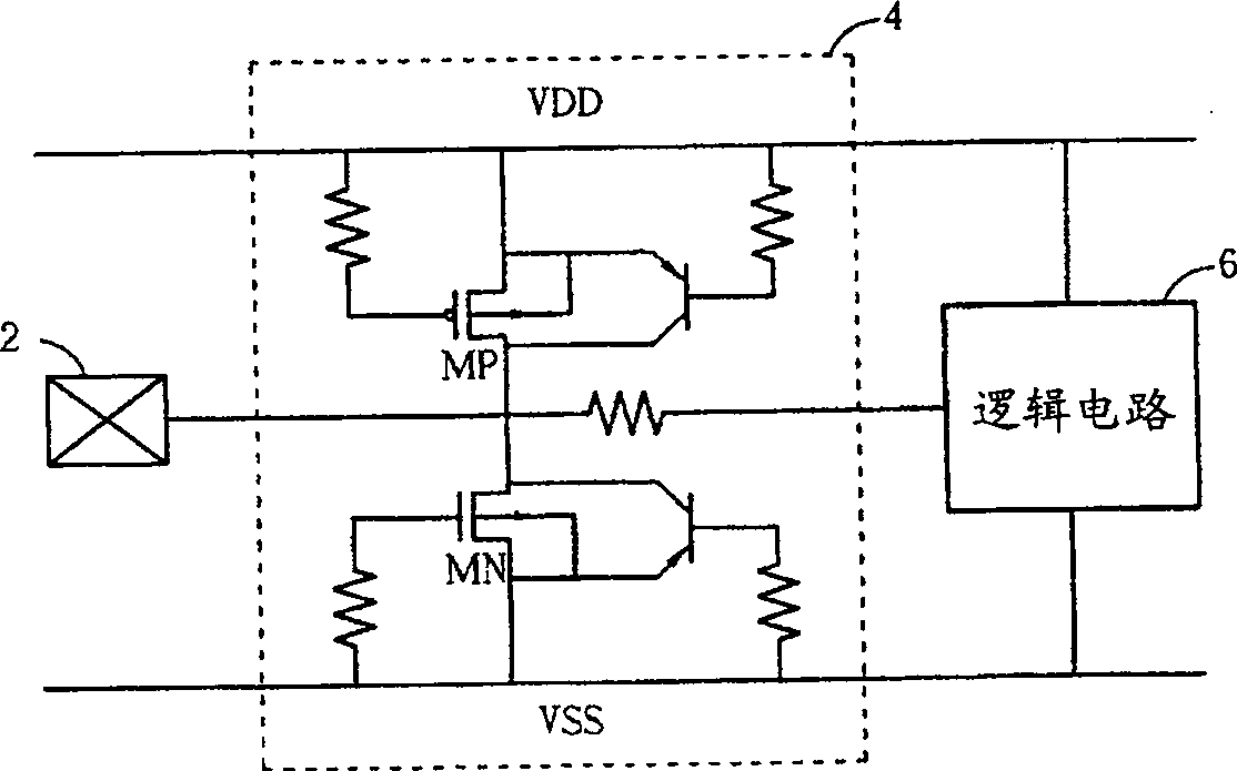
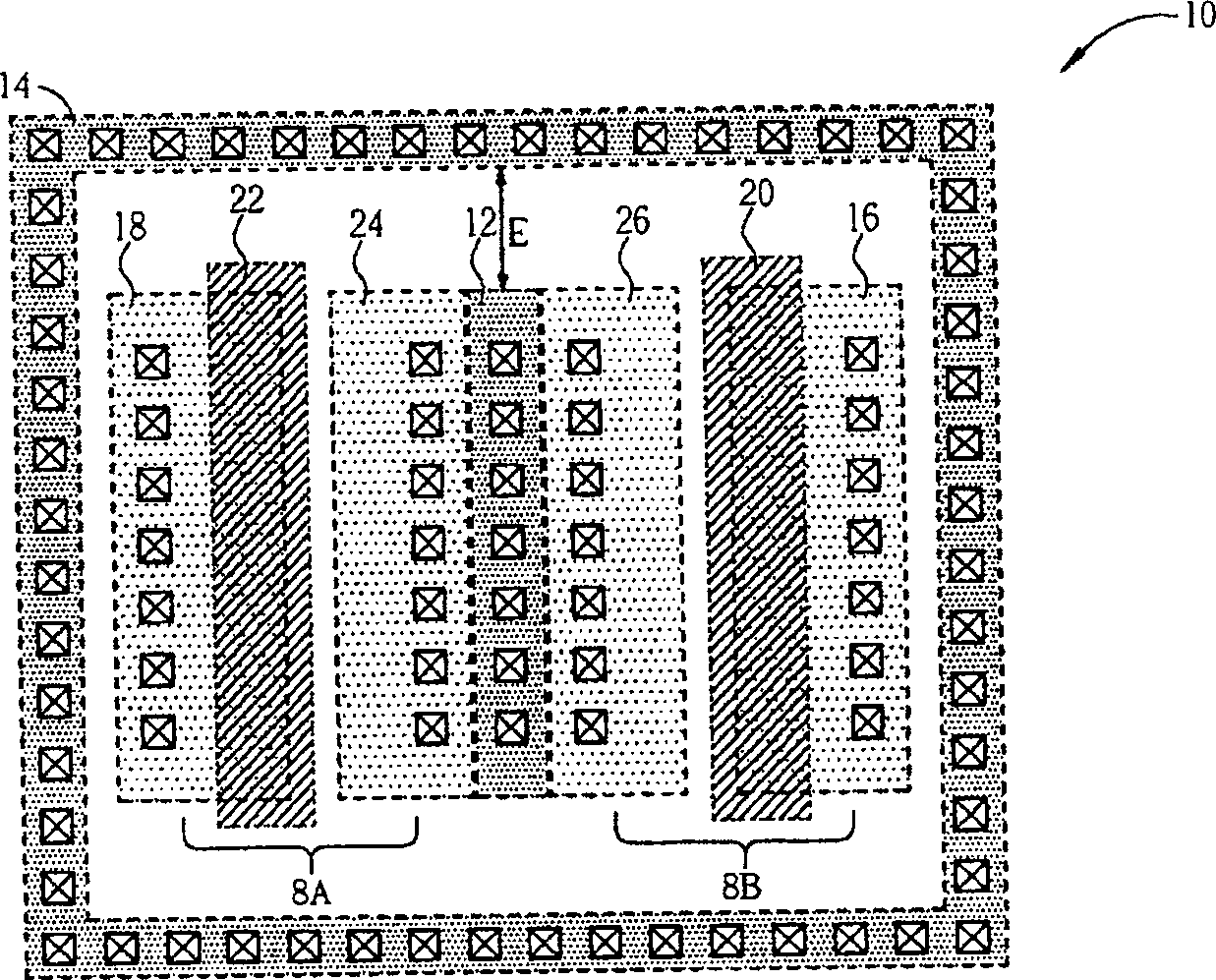
technical field [0001] The invention provides a transistor layout method, especially a transistor layout method that can improve electrostatic tolerance. Background technique [0002] As the dimensions of transistor components continue to shrink, the junction between the source and drain of transistors becomes shallower and the thickness of the gate oxide layer becomes thinner. When the thickness of the gate oxide layer becomes thinner and the breakdown voltage of the diode junction transistor decreases, the transistor is easily damaged by electrostatic discharge (ESD), so each pin of the base circuit chip needs to be protected by ESD protection components , and then connected to the internal wiring. [0003] see figure 1 , figure 1 It is a schematic diagram of an existing protective element 4 . One end of the protection element 4 is connected to a pad 2 and the other end is connected to a logic circuit 6 . When a large amount of electrostatic charge flows into the cont...

Claims


Application Information

Patent Timeline
Patent Type & Authority Patents(China)
IPC IPC(8): H01L27/088H01L23/60H01L21/8234
Inventor 余锦旗杨毓儒陈志熹黄启模
Owner ILI TECHNOLOGY CORPORATION
Learn More