Laser ablation tape for solder interconnect formation

a technology of solder interconnect and laser ablation tape, which is applied in the direction of semiconductor devices, semiconductor/solid-state device details, electrical apparatus, etc., can solve the problems of microelectronic device yield loss, reliability issues, and continuous effort to improve these processes

Active Publication Date: 2014-11-13
INTEL CORP
View PDF5 Cites 2 Cited by
  • Summary
  • Abstract
  • Description
  • Claims
  • Application Information

AI Technical Summary

Problems solved by technology

The smaller size and pitch of the attachment structures makes them more susceptible to damage from fabrication processes, which may result in reliability issues and yield loss for the microelectronic devices.
Thus, there is a continual effort to improve these processes.

Method used


Image

  • Laser ablation tape for solder interconnect formation
  • Laser ablation tape for solder interconnect formation
  • Laser ablation tape for solder interconnect formation

Examples


example 12

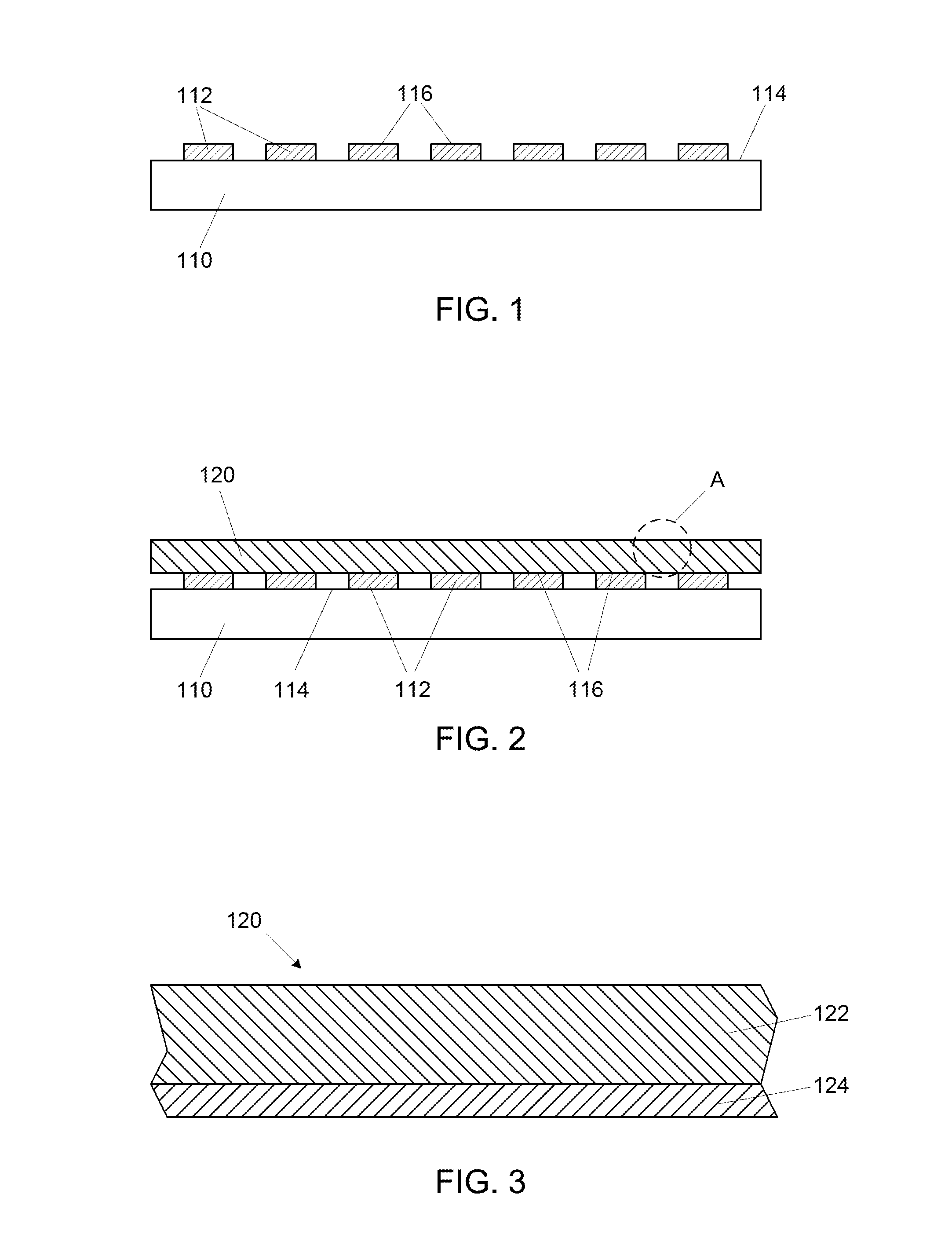
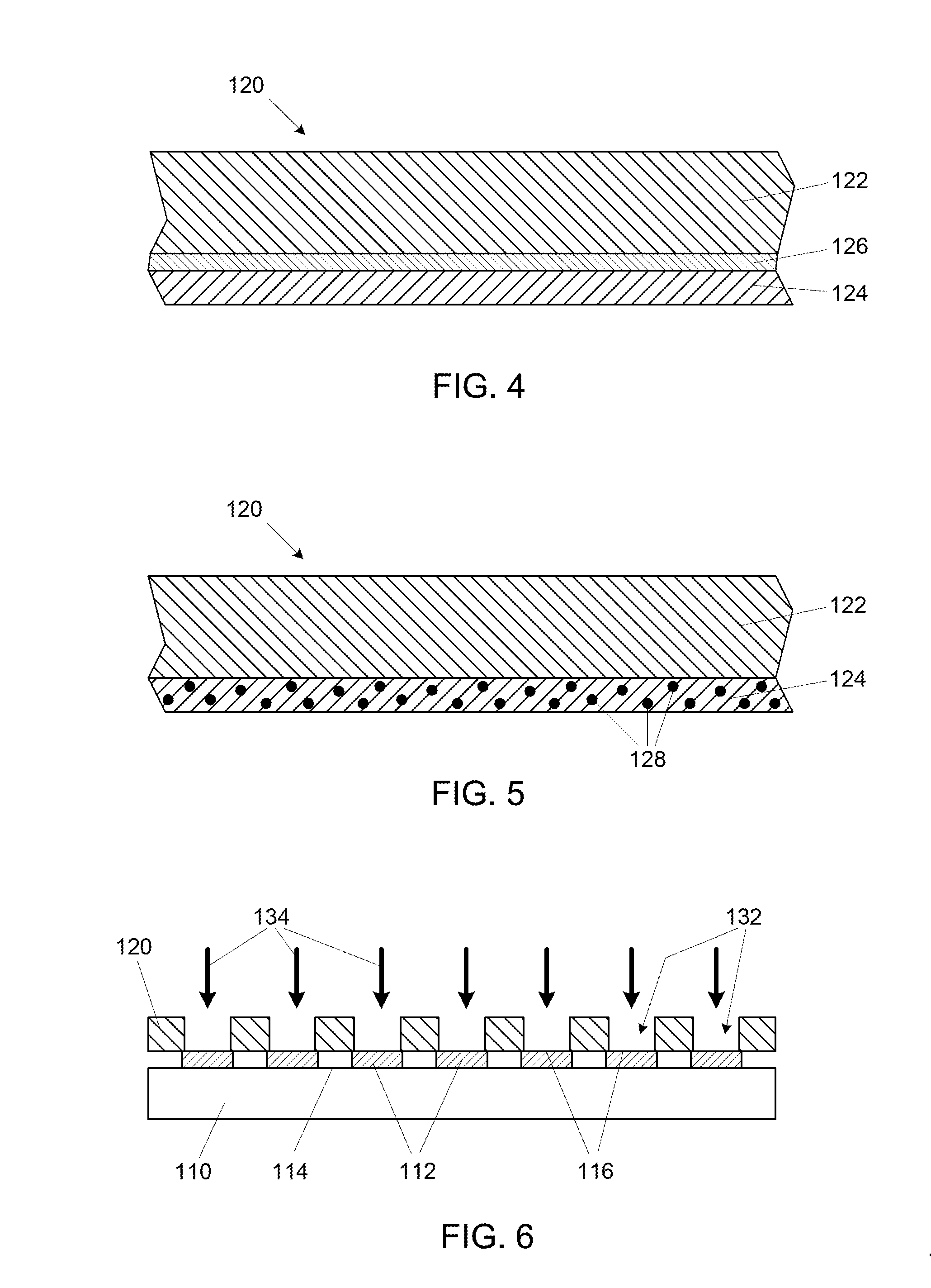
[0037]In Example 12, the subject matter of any of Examples 10 to 11 can optionally include attaching the laser ablation tape to the at least one bond pad comprising forming the laser ablation tape by providing a base film and disposing an adhesive layer on the base film; and attaching the laser ablation tape to the at least one bond pad with the adhesive layer.

[0038]In Example 13, the subject matter of any of Example 10 to 11 can optionally include attaching a laser ablation tape to the at least one bond pad comprising forming the laser ablation tape by providing a base film, disposing an electrostatic discharge layer on the base film, and disposing an adhesive layer on the static discharge layer, and attaching the laser ablation tape to the at least one bond pad with the adhesive layer.

[0039]In Example 14, the subject matter of Example 13 can optionally include disposing the electrostatic discharge layer on the base film comprising disposing a conductive polymer on the base film.

[0...


PUM


Abstract

A tape capable of laser ablation may be used in the formation of microelectronic interconnects, wherein the tape may be attached to bond pads on a microelectronic device and vias may be formed by laser ablation through the tape to expose at least a portion of corresponding bond pads. The microelectronic interconnects may be formed on the bond pads within the vias, such as by solder paste printing and solder reflow. The laser ablation tape can be removed after the formation of the microelectronic interconnects.

Description

TECHNICAL FIELD[0001]Embodiments of the present description generally relate to the fabrication of solder interconnects of a microelectronic device, and, more specifically, to using a tape capable of laser ablation to form microelectronic interconnects.BACKGROUND ART[0002]The microelectronic industry is continually striving to produce ever faster and smaller microelectronic devices for use in various mobile electronic products, such as portable computers, electronic tablets, cellular phones, digital cameras, and the like. As these goals are achieved, the size of attachment structures, such as microelectronic interconnects for the microelectronic devices, and the space or pitch between these attachment structures becomes smaller. The smaller size and pitch of the attachment structures makes them more susceptible to damage from fabrication processes, which may result in reliability issues and yield loss for the microelectronic devices. Thus, there is a continual effort to improve thes...

Claims


Application Information

Patent Timeline
Patent Type & Authority Applications(United States)
IPC IPC(8): H01L23/00
CPCH01L24/11H01L2224/11632H01L24/03H01L24/05H01L24/13H01L21/6835H01L2224/03845H01L2224/0391H01L2224/05571H01L2224/05624H01L2224/05647H01L2224/11442H01L2224/11849H01L2224/1191H01L2224/13023H01L2224/13111H01L2224/13116H01L2224/05568H01L2224/11474H01L2924/12042H01L2224/0401H01L2224/1134H01L2924/013H01L2924/00014H01L2924/0105H01L2924/00012H01L2924/00
Inventor BRUN, XAVIER F.KUMAMOTO, TAKASHIAHMED, SUFI
Owner INTEL CORP
Why Eureka
Try Eureka