Adaptive Local Threshold and Color Filtering

a local threshold and color filtering technology, applied in the field of detecting defects on wafers, can solve problems such as users' need to change the wafer inspection process, process generally detects a significant amount of potential defects, and nuisance defects

Active Publication Date: 2015-02-12
KLA TENCOR TECH CORP
View PDF8 Cites 17 Cited by
  • Summary
  • Abstract
  • Description
  • Claims
  • Application Information

AI Technical Summary

Benefits of technology

[0011]One embodiment relates to a computer-implemented method for detecting defects on a wafer. The method includes determining local statistics of pixels in output for a wafer generated using an inspection system. The method also includes determining which of the pixels are outliers based on the local statistics. The method further includes comparing the outliers to the pixels surrounding the outliers to identify the outliers that do not belong to a cluster of outliers as defect candidates. In addition, the method includes determining a value for a difference in color between the pixels of the defect candidates and the pixels surrounding the defect ca

Problems solved by technology

However, as the dimensions of semiconductor devices decrease, inspection becomes even more important to the successful manufacture of acceptable semiconductor devices because smaller defects can cause the devices to fail.
Inspection processes generally detect a significant amount of potential defects that are actually nuisance defects on the wafer or noise.
For instance, nuisance defects may be events that are detected as defects but are actually color variations in images of a wafer due to variations in a process performed on the wafer that do not have any effect on the devices being fabricated on the wafer.
Therefore, detecting such nuisance defects and reporting them as actual defects to a user have a number of disadvantages such as obscuring actual defects that a user cares about and/or affect the device fabrication in a meaningful manner in the inspection results, obstructing process control attempts to correct the actual def

Method used


Image

  • Adaptive Local Threshold and Color Filtering
  • Adaptive Local Threshold and Color Filtering
  • Adaptive Local Threshold and Color Filtering

Examples


Embodiment Construction

[0020]Turning now to the drawings, it is noted that the figures are not drawn to scale. In particular, the scale of some of the elements of the figures is greatly exaggerated to emphasize characteristics of the elements. It is also noted that the figures are not drawn to the same scale. Elements shown in more than one figure that may be similarly configured have been indicated using the same reference numerals. Unless otherwise noted herein, any of the elements described and shown may include any suitable commercially available elements.

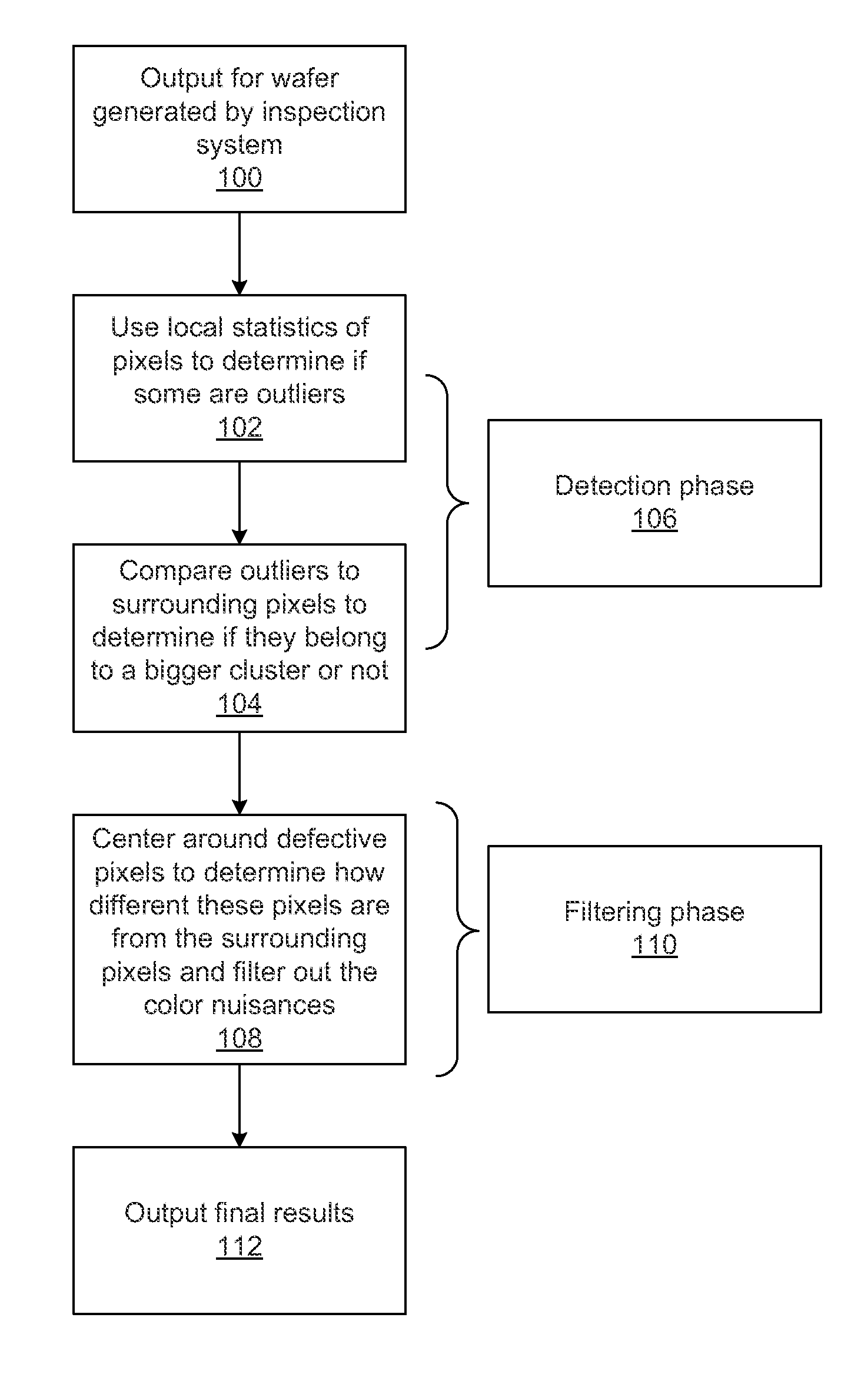
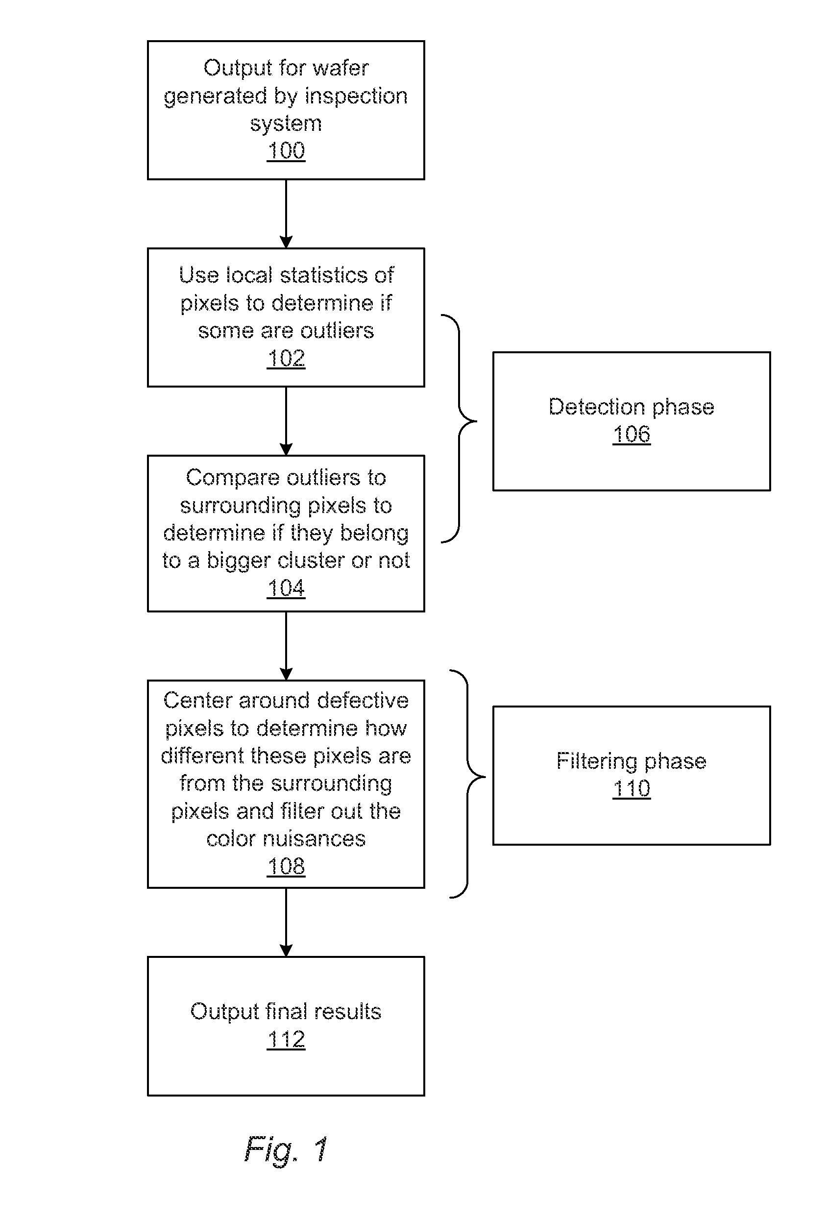
[0021]One embodiment relates to a computer-implemented method for detecting defects on a wafer. As is described in detail further herein, the embodiments use adaptive local thresholds and color filtering to detect defects on wafers.

[0022]The method includes determining local statistics of pixels in output for a wafer generated using an inspection system. The computer-implemented method may include acquiring the output using the inspection system. For...


PUM


Abstract

Methods and systems for detecting defects on a wafer using adaptive local thresholding and color filtering are provided. One method includes determining local statistics of pixels in output for a. wafer generated using an inspection system, determining which of the pixels are outliers based on the local statistics, and comparing the outliers to the pixels surrounding the outliers to identify the outliers that do not belong to a cluster of outliers as defect candidates. The method also includes determining a value for a difference in color between the pixels of the defect candidates and the pixels surrounding the defect candidates. The method further includes identifying the defect candidates that have a value for the difference in color greater than or equal to a predetermined value as nuisance defects and the defect candidates that have a value for the difference in color less than the predetermined value as real defects.

Description

BACKGROUND OF THE INVENTION[0001]1. Field of the Invention[0002]This invention generally relates to detecting defects on a wafer using adaptive local thresholding and color filtering.[0003]2. Description of the Related Art[0004]The following description and examples are not admitted to be prior art by virtue of their inclusion in this section.[0005]Inspection processes are used at various steps during a semiconductor manufacturing process to detect defects on wafers to promote higher yield in the manufacturing process and thus higher profits. Inspection has always been an important part of fabricating semiconductor devices such as ICs. However, as the dimensions of semiconductor devices decrease, inspection becomes even more important to the successful manufacture of acceptable semiconductor devices because smaller defects can cause the devices to fail.[0006]Inspection processes generally detect a significant amount of potential defects that are actually nuisance defects on the wafe...

Claims


Application Information

Patent Timeline
IPC IPC(8): G06T7/00G06T7/40
CPCG06T7/0008G06T2207/20024G06T2207/30148G06T7/408G06T7/0006G06T2207/10024G06T2207/20076G06T7/90
Inventor HUANG, JUNQINGLEE, HUCHENGWU, KENONGGAO, LISHENG
Owner KLA TENCOR TECH CORP
Why Eureka
Try Eureka