Eureka AIR delivers breakthrough ideas for toughest innovation challenges, trusted by R&D personnel around the world.

Atom probe tomography sample preparation for three-dimensional (3D) semiconductor devices

a three-dimensional (3d) semiconductor and atom probe technology, applied in individual semiconductor device testing, semiconductor/solid-state device testing/measurement, instruments, etc., can solve the problems of device or structure damage, performance characteristics shift, etc., to achieve the effect of minimizing the amorphization of the surface of the crystalline surfa

Active Publication Date: 2015-06-11
IBM CORP
View PDF6 Cites 10 Cited by
  • Summary
  • Abstract
  • Description
  • Claims
  • Application Information

AI Technical Summary

Benefits of technology

[0006]According to at least one exemplary embodiment, a method for atom probe tomography (APT) sample preparation from a three-dimensional (3D) field effect transistor device formed within a semiconductor structure is provided. The method may include measuring a capacitance-voltage (C-V) characteristic for the 3D field effect transistor device; identifying, based on the measured capacitance-voltage (C-V) characteristic, a Fin structure corresponding to the 3D field effect transistor device; detaching the identified Fin structure from the 3D field effect transistor device using a nanomanipulator probe tip; welding the detached Fin to the nanomanipulator probe tip using an incident focused ion beam having a voltage of less than about 1000 eV; and applying the incident focused ion beam having a voltage of less than about 1000 eV to a tip of the Fin that is welded to the nanomanipulator probe tip. The tip of the Fin may be sharpened by the focused ion beam.
[0007]According to at least one other exemplary embodiment, a method for atom probe tomography (APT) sample preparation from a three-dimensional (3D) field effect transistor device formed within a semiconductor structure is provided. The method may include applying a voltage in the range of about 50 eV to less than 300 eV to an inductively coupled Argon ion source operating at a radio frequency; generating, from the Argon ion source, a collimated ion beam incident on a crystalline surface of the semiconductor structure for planar removal of layers of the crystalline surface, whereby the collimated ion beam minimizes surface amorphization of the crystalline surface of the semiconductor structure; exposing first and second contact regions underlying the crystalline surface associated with the 3D field effect transistor device using an end-point detector based on the planar removal of the layers; coupling a high-frequency impedance probe having a frequency range of about 5 Mhz to about 110 Mhz to an impedance analyzer; coupling the high-frequency impedance probe to a first and a second atomic force probe tip; coupling, using an atomic force microscope, the first atomic force probe tip to the exposed first contact region; coupling, using the atomic force microscope, the second atomic force probe tip to the exposed second contact region; measuring the C-V characteristic for the 3D field effect transistor device on the impedance analyzer, the impedance analyzer applying an operating frequency corresponding to the frequency range of about 5 Mhz to about 110 Mhz to the first and second contact regions associated with the 3D field effect transistor device using the high-frequency impedance probe; and detaching, based on the measured C-V characteristic, a Fin structure from the 3D field effect transistor device using a nanomanipulator probe tip, the detached Fin being both welded to the nanomanipulator probe tip and shaped using an incident focused ion beam having a voltage of less than about 1000 eV.

Problems solved by technology

Such delayering techniques may, however, damage the device or structure's surface, or alternatively, introduce unwanted irregularities (e.g., unwanted ion implantation) into the device or structure.
For example, the process used to prepare the device or structure prior to test or evaluation may undesirably introduce defects (e.g., gallium ion implantations due to high energy ion beam etching) or produce shifts in performance characteristics (e.g., MOSFET threshold voltage (Vt) shifts).

Method used


Image

  • Atom probe tomography sample preparation for three-dimensional (3D) semiconductor devices
  • Atom probe tomography sample preparation for three-dimensional (3D) semiconductor devices
  • Atom probe tomography sample preparation for three-dimensional (3D) semiconductor devices

Examples


Embodiment Construction

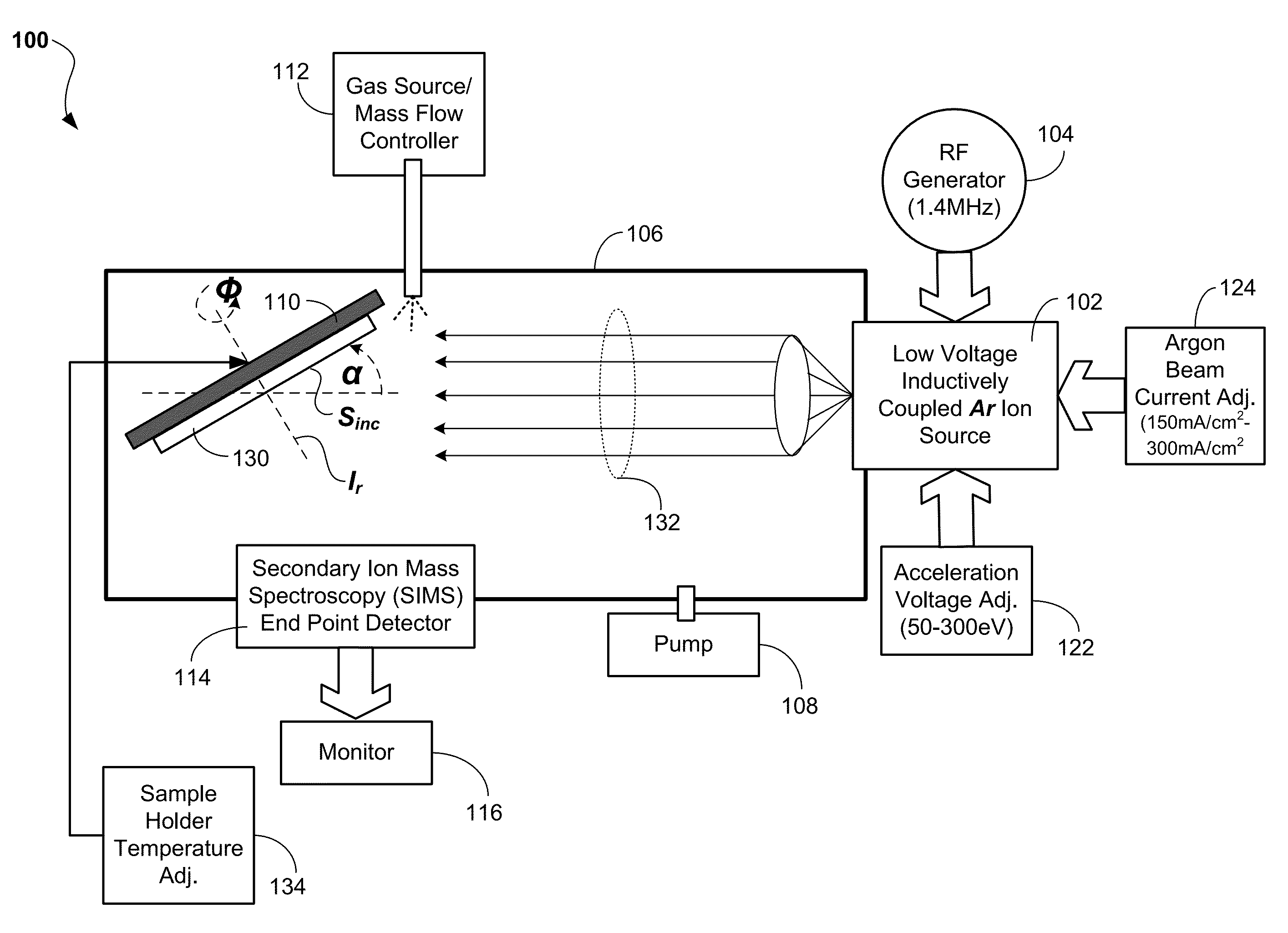
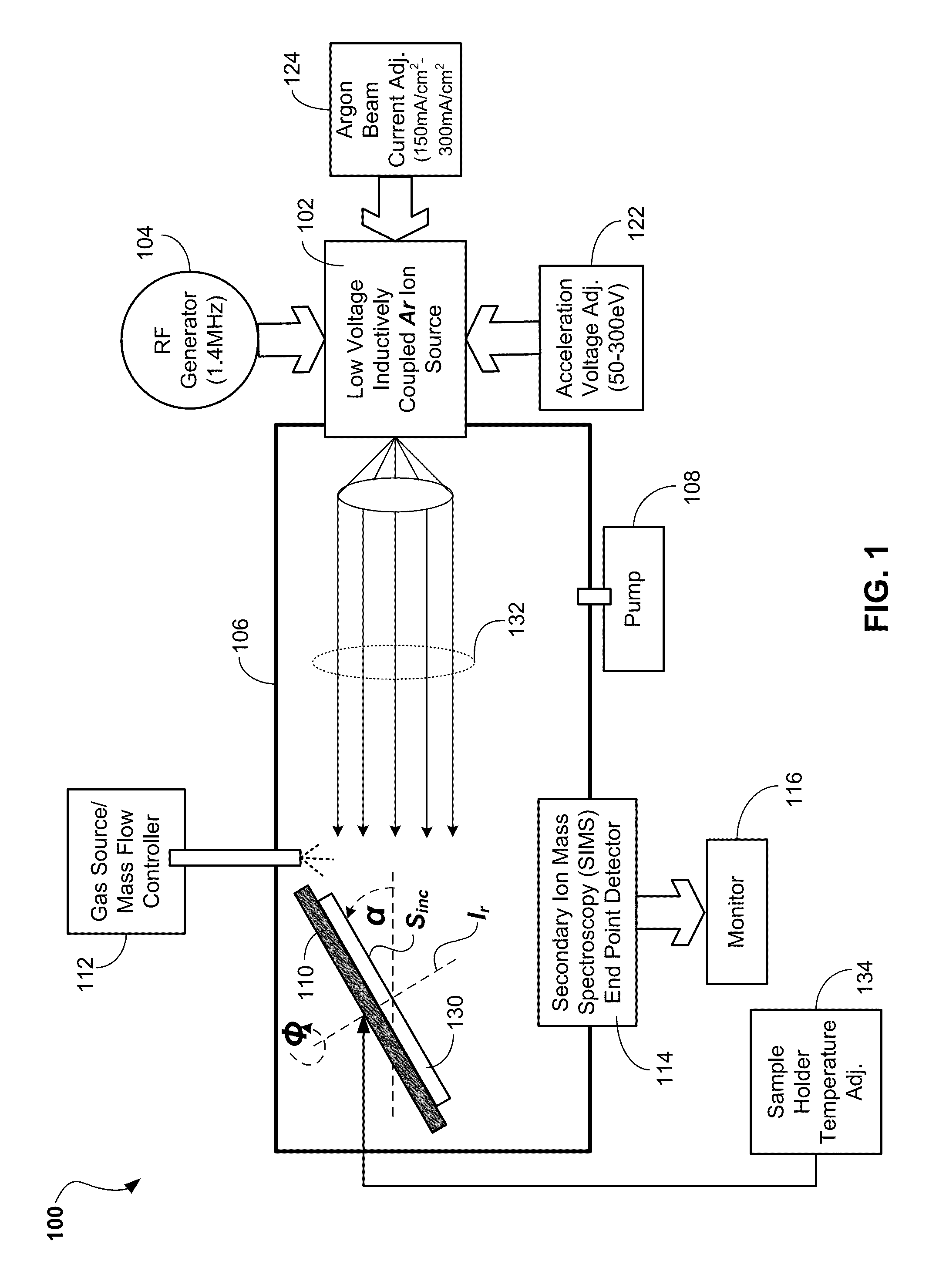
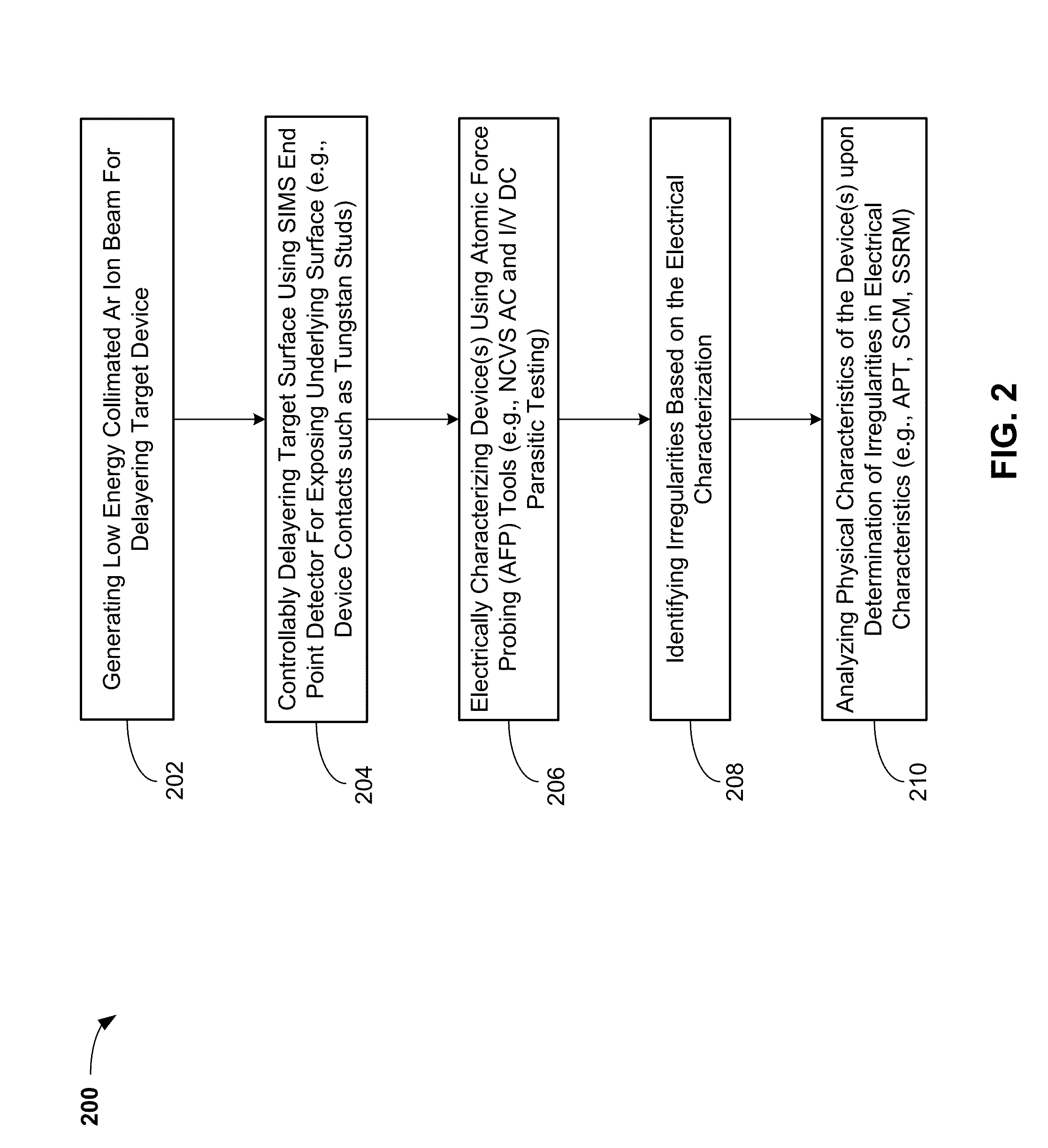
[0021]The following one or more exemplary embodiments describe, among other things, a low energy ion beam milling apparatus and method utilized for the purpose of delayering the surfaces of semiconductor devices for subsequent testing and characterization of such devices. The delayering of various surfaces of semiconductor devices, particularly three-dimensional semiconductor devices such as discrete FinFet transistor devices, may inadvertently introduce defects and unwanted artifacts within the devices. For example, a high-energy 500 eV focused gallium ion beam may, during the milling and delayering process of a FET device, cause a shift in the threshold voltage (Vt) of the FET device. Additionally, the high-energy ion beam may alter dopant density or dopant distribution. In all such cases, the device may be characterized incorrectly as a result of the induced irregularities or defects that are inadvertently introduced into the semiconductor device under tests based on the ion beam...


PUM


Abstract

A method for atom probe tomography (APT) sample preparation from a three-dimensional (3D) field effect transistor device formed within a semiconductor structure is provided. The method may include measuring a capacitance-voltage (C-V) characteristic for the 3D field effect transistor device and identifying, based on the measured capacitance-voltage (C-V) characteristic, a Fin structure corresponding to the 3D field effect transistor device. The identified Fin structure is detached from the 3D field effect transistor device using a nanomanipulator probe tip. The detached Fin is then welded to the nanomanipulator probe tip using an incident focused ion beam having a voltage of less than about 1000 eV. The incident focused ion beam having a voltage of less than about 1000 eV is applied to a tip of the Fin that is welded to the nanomanipulator probe tip. The tip of the Fin may then be sharpened by the focused ion beam.

Description

BACKGROUND[0001]a. Field of the Invention[0002]The present invention generally relates to semiconductor device testing, and more particularly, to the preparation of a device under test (DUT) during such semiconductor device testing.[0003]b. Background of Invention[0004]Semiconductor device performance may be measured using a myriad of techniques and instruments. For example, in order to perform Atomic Force Probing (AFP) of a semiconductor device or structure, various layers may need to be removed for exposing the device or structure's contacts (e.g., tungsten studs) or surface prior to probing. Such layer removal or delayering may be carried out using either more coarse methods such as chemical mechanical polishing (CMP) or relatively high-precision techniques employing, for example, focused or collimated high-energy (>500 eV) ion beam etching. Such delayering techniques may, however, damage the device or structure's surface, or alternatively, introduce unwanted irregularities (...

Claims


Application Information

Patent Timeline
Patent Type & Authority Applications(United States)
IPC IPC(8): G01R31/26G01Q30/20H01J37/317
CPCH01J2237/31749G01R31/2644G01Q30/20H01J37/317G01R31/2621G01N1/32G01Q60/40G01R31/2898H01L22/14H01L22/20
Inventor KANE, TERENCE L.WALSH, JOHN M.
Owner IBM CORP
Why Eureka
Eureka Blog
Learn More