Array substrate and preparation method thereof, display panel and display device
- Summary
- Abstract
- Description
- Claims
- Application Information
AI Technical Summary
Benefits of technology
Problems solved by technology
Method used
Image

Examples
Embodiment Construction
[0017]The implementation processes of the embodiments of the present invention will be illustrated in detail below in combination with drawings of the description. It should be noted that the same or similar signs express the same or similar components or components with the same or similar functions throughout. The embodiments described with reference to the drawings below are exemplary, and are merely used for interpreting the present invention, rather than limiting the present invention.
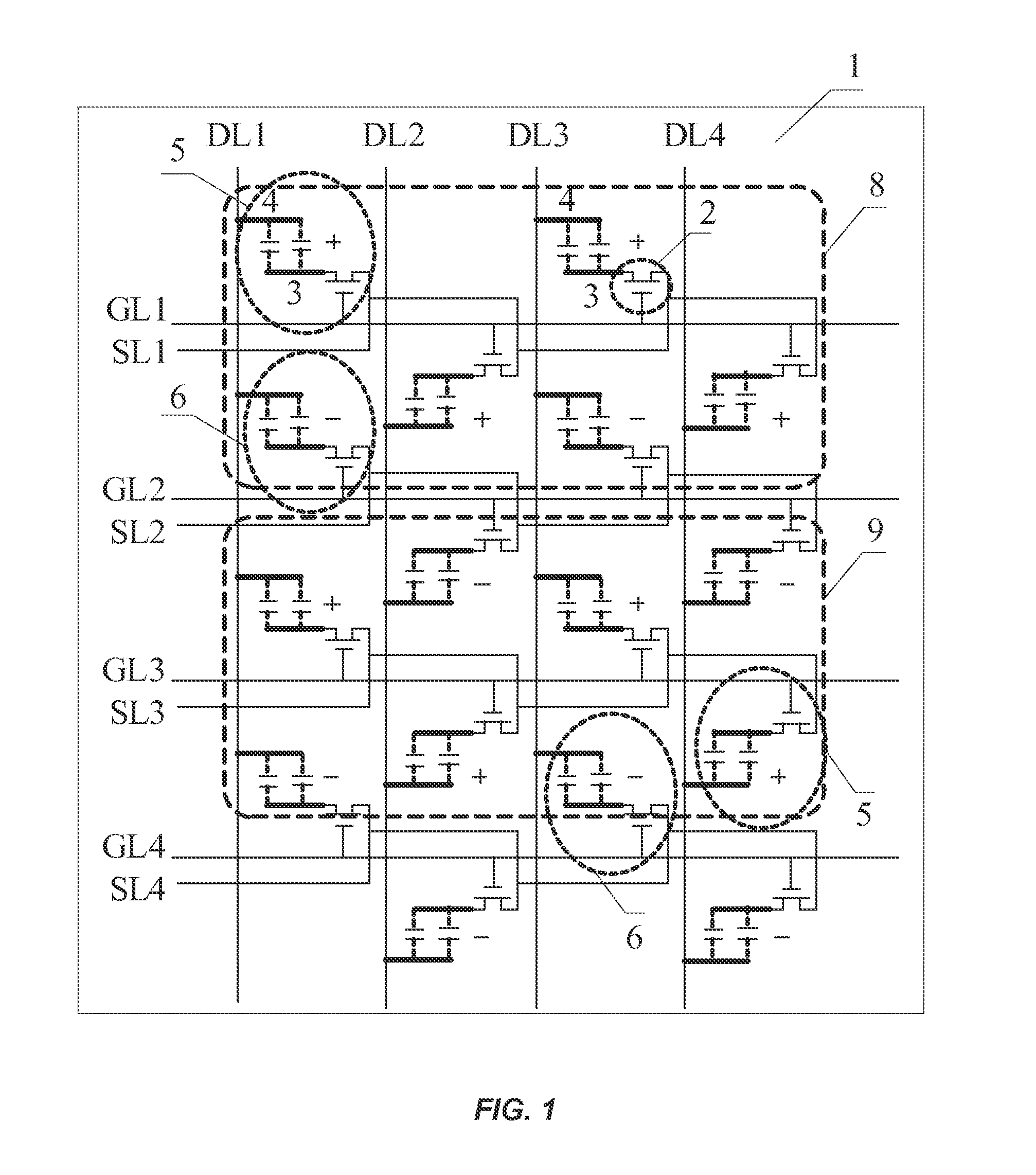
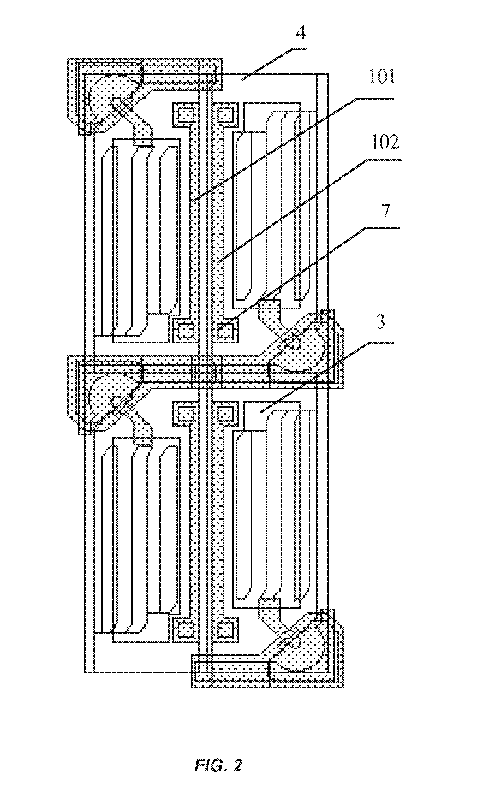
[0018]As shown in FIG. 1, an embodiment of the present invention provides an array substrate, including a substrate 1, an array of pixel units defined by a plurality of gate lines and a plurality of data lines crossed on the substrate 1, and a plurality of common electrode lines; the gate lines are GL1, GL2, GL3 or GL4 arranged between two adjacent rows of pixel units as shown in FIG. 1; the data lines are DL1, DL2, DL3 or DL4 as shown in FIG. 1; and the common electrode lines are SL1, SL2, SL3 or...
PUM
 Abstract
Description
Claims
Application Information